First post, by Anonymous Coward

- Rank
- l33t++
This thread is to be used to report my findings with a VL/EISA Socket4 Pentium system I've been playing with. I am very interested in playing with expensive high-end toys and PC upgrades available in the 1992-1994 time frame. In this case, VL-BUS, EISA and Socket4 Pentiums. It's something hard to appreciate unless you were into PCs at that time. In 1993 the Pentium held near mythical status, and there was still uncertainty about which 32-bit card expansion bus was the way of the future. This is why this ridiculous motherboard exists (it's one of perhaps only 2 or 3 to feature both EISA and VL-bus with a Pentium CPU):
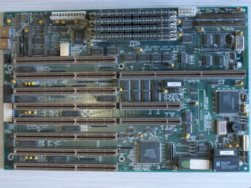
This is the Acer J3 active backplane motherboard. It mainly featured in the the Acer Power and Acros line of computers, but was also found in other OEM systems like AMBRA, Apricot and perhaps a few Japanese makes as well. Several different CPU cards are available: single socket3, single socket4, dual socket4, single socket5 and dual socket5. As far as I know they are all based around OPTi chipsets, though I did hear a rumor a Triton board may exist.
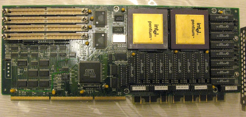
I own the dual socket4 card. Mine came with two mismatched P60s. One has FDIV and the other does not. They do not have the same sspecs. I am not sure how well it would work in an SMP enabled OS. Since I do not have the matching heatsinks for these chips (I don't want to use epoxy) I am unable to find out. In the mean time I have replaced these two CPUs with a single PODP5V133 upgrade chip. I replaced the oscillator with a 66MHz part to get the full 133MHz. The board has silk screen indicating support for 80MHz FSB, but I have not yet been brave enough to try it out. The card also supports 1MB L2 cache. I am not sure if this card does bank interleave, and I haven't bothered to test the 1MB setting yet (though I do have the chips to do so).
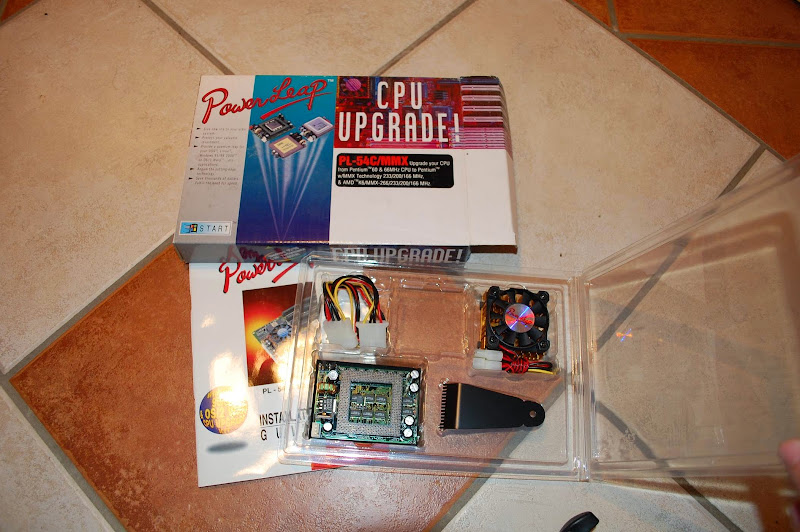
Performance of this board is not all that great. CPU marks are about where they should be, but the DRAM throughput is kind of shite. This is pretty consistent with most of the OPTi based boards I've tried for 386 and 486 systems. This appears to be a jerry rigged 486 design. My SiS EISA board eats this thing for lunch in this regard. However, I am hoping perhaps I can get a main memory performance boost by using a CPU with integrated L2 cache. This is possible using an adapter like this one. It's currently en-route from Germany. (Thanks to 386_Junkie for this one). I will post benchmark results when available.
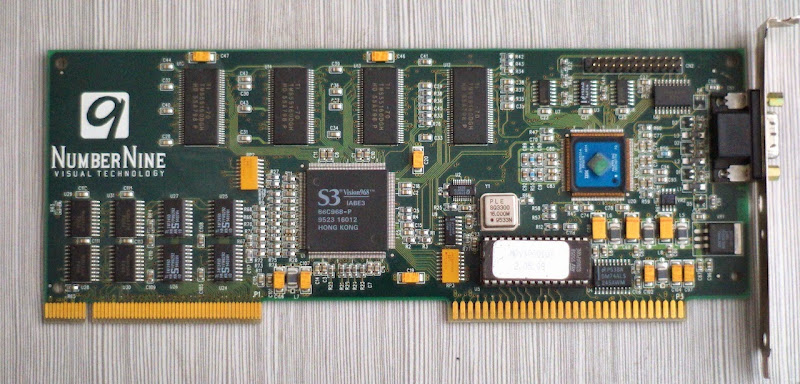
For VGA I have settled on #9 Motion FX 771 with 4MB VRAM. This is just about top of the line for VLB. Somehow I only managed to pay a few dollars for this card. This card is somewhat special for a VLB card because of the 220MHz RAMDAC and the VRAM which is mounted on both sides of the PCB. I attempted to run et4000W32P in my system as well, but neither of my cards would power up. This was the same problem I had in my previous OPTi based VLB Pentium system.
My disk system will comprise of an Adaptec AHA-2742W EISA based wide SCSI adapter. This one is fairly basic, but it's my understanding that caching controllers on EISA systems with lots of memory are somewhat useless. My motherboard supports up to 512MB of FPM DRAM with the CPU card I have, and I currently have 256MB installed, so I figured it should be more than enough to keep things running smoothly. The drive I will be using is a Quantum/Maxtor Atlas IV 36GB (10k).

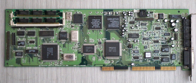
A stupidly complex computer deserves a stupidly long and complex soundcard. AWE32 is pretty much the perfect match. They were also stupidly expensive when they were knew. It's just a pity I sold the original CT2760 card several years back. The CT3990 is close enough though. Not sure if I will use a daughter board or not. Probably not worth the hassle in light of the hanging note bug.
Not sure what other toys will go in this system at the moment. For now it doesn't have a dedicated chassis and I've stolen the Inwin H500 from my EISA 486 build. It will likely be another ATX conversion though.
"Will the highways on the internets become more few?" -Gee Dubya
V'Ger XT|Upgraded AT|Ultimate 386|Super VL/EISA 486|SMP VL/EISA Pentium


 but with a different measurement.