VOGONS


First post, by Ketturi

User metadata
Rank Newbie
Rank
Newbie

Lets plunge directly into the deep end with my first forum post here.
Recently, I managed to get my hands on the vintage Olivetti Echos 44 laptop from 1994. This little gem is equipped with a 486 CPU, 12MB of RAM, a 350MB hard drive, a floppy drive, and PCMCIA expansion slots. However, luck wasn't on my side as the hard drive had seen better days. It caused all sorts of issues - reporting itself as a 1TB drive meant for modern computers, constant lock-ups, and overall unhappiness.

The previous owner had installed Windows 95, but luckily, most of the old system files were intact and I was able to extract them, fortunately, because I couldn't find these files anywhere on the internet. So, I took the normal route and replaced the hard drive with a CF card IDE adapter. However, there were additional challenges. The BIOS had a 504MB hard limit, and Olivetti used the hard drive for a hidden recovery partition containing minimal DOS boot files and a file for hibernating the system when APM is enabled. This made it difficult to use OnTrack or Ez-Drive managers, as they interfered with the hidden partition and hibernation region.

That's when I had the idea to try XTIDE Universal BIOS, hoping it would provide support for larger drives and modern CF cards. So, I started researching how to add it to the system.

Echos 44 has 28F020 flash rom for the video bios, extended bios that contains PhoenixMISER, and system bios. Not all parts of the flash rom are used, as it starts from the C000h segment with video bios, and continues
to the end of the address space. Chipset on board handles the address decoding for the flash rom, and has registers to enable or disable parts of the flash rom decoding. It also handles shadow ram and caching functionality.

Chipset in question is OPTi 82C463 single chip notebook IC. Databook for this can be found from the internet, and I have copy of it here https://ketturi.kapsi.fi/Echos44/82C463.pdf
I unsoldered the SMD bios chip, and replaced it with socket on the CPU card, and dumped bios for disassembly. I attached the dump here, and it can also be found from the https://ketturi.kapsi.fi/Echos44/ folder.
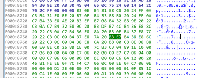
Now with the bios dump, I could load it in the IDA Freeware, and start disassemble and explore the bios. Quite early I found part that loads the chipset registers from the table in the bios rom.

chipset%20register%20loading.PNG
https://ketturi.kapsi.fi/Echos44/config_chipset.asm
And it loads this table to the chipset registers:

db 30h          ; DATA XREF: BOOT-D0↑o
; Control Register 1
db 00101010b ; 0 Revision
; 0 Revision
; 1 RIing in enanbled
; 0 Turbo VGA disabled
; 1 Global Reloc/Trans enabled for SMI addresses
; 0 no extra AT wait state
; 1 Fast Reset control does not require Halt
; 0 Always write 0!
db 31h
; Control Register 2
db 01101111b ; 0 Master byte swap disable
; 1 Reserved
; 1 Parity check Disable
; 0 Dynamic SMI relocation disabled
; 1 EC000h Control ROMCS
; 1 E8000h Control ROMCS
; 1 E4000h Control ROMCS
; 1 E0000h Control ROMCS
db 32h
; Shadow RAM Control Register 1
db 11100101b ; 1 F0000h control, ROMCS
; 1 Reserved Awlays 1
; 1 Reserved Always 1
; 0 D0000h block shadow write, writable
; 0 E0000h block shadow write, writable
; 1 Reserved
; 0 Reserved (awlays write 0)
; 1 Single ALE druing bus conversion
db 33h
; Shadow RAM Control Register 2
db 00000000b ; Disable E0000 and D0000 shadow ram
db 34h
; DRAM Control Register 1
db 10001101b ; Bank 0 1M
; Bank 1 x
; Bank 2 x
; Bank 3 x
db 35h
; DRAM Control Register 2
db 10010111b ; 10 DRAM R wait states: 1, 3-2-2-2
; 01 DRAM W wait states: 1
; 0 MP2/STRAP2: 2x Clock (read only)
; 1 F0000h non-cacheable
; 1 All DRAM is not cacheable
; 1 C0000h non-cacheable
db 36h
; Shadow RAM Control Register 3
db 10010000b ; 1 F0000 block wrote to ROMCS#
; 0 C0000-EFFFF R/W From AT bus or ROMCS
; 0 C0000 block shadow writable
; 1 Reserved, Alaways write 1
; 0 Shadow CC000 disable
; 0 Shadow C8000 disable
; 0 Shadow C4000 disable
; 0 Shadow C0000 disable
db 37h
; E0000h Block Cache Enable Bits Register
db 11111111b ; DC000 ROMCS
Show last 29 lines
				; D8000 ROMCS
; D4000 ROMCS
; D0000 ROMCS
; EC000 non-cacheable
; E8000 non-cacheable
; E4000 non-cacheable
; E0000 non-cacheable
db 38h
; Non-cacheable Block 1 Register
db 10000110b ; 1 Size of non-cacbeable memory block:
; 0 100=Disabled
; 0
; 0 CC000-CFFFF AT-BUS
; 0 C8000-CBFFF AT-BUS (Change these to enable C800 romcs)
; 1 C4000-C7FFF ROMCS#
; 1 C0000-C3FFF ROMCS#
; 0 Address bit A24 of non-cacheable memory block1
db 39h
; Non-Cacheable Block 1 Register 2
db 00000000b ; Default
db 3Ah
; Non-Cacheable Block 2 Register 1
db 00000000b ; Default
db 84h
; What is this!!!
db 00000000b ; Default
db 3Bh
; Non-Cacheable Block 2 Register 2
db 00000000b ; Default

At first glance, this seemed too easy to be true, and as expected, it wasn't that simple. This is not the only part where the registers handling the ROM decoding are modified. Due to the shadow RAM and caching, there is another function that sets the register values and copies the content of the ROM to the shadow RAM. Otherwise, I could have simply flashed the XTIDE to either the C800h or D000h region, changed those segments from AT-BUS to ROMCS# decoding, and been done with it.

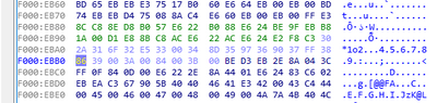
Here is the tricky part I have been struggling with, and I would appreciate some help. I identified the subfunction that handles the shadow RAM operations for the option ROMs:
https://ketturi.kapsi.fi/Echos44/shadowram.asm
In the beginning of the function, the chipset registers are set for copying the option ROM data to the DRAM:
shadowram1.PNG

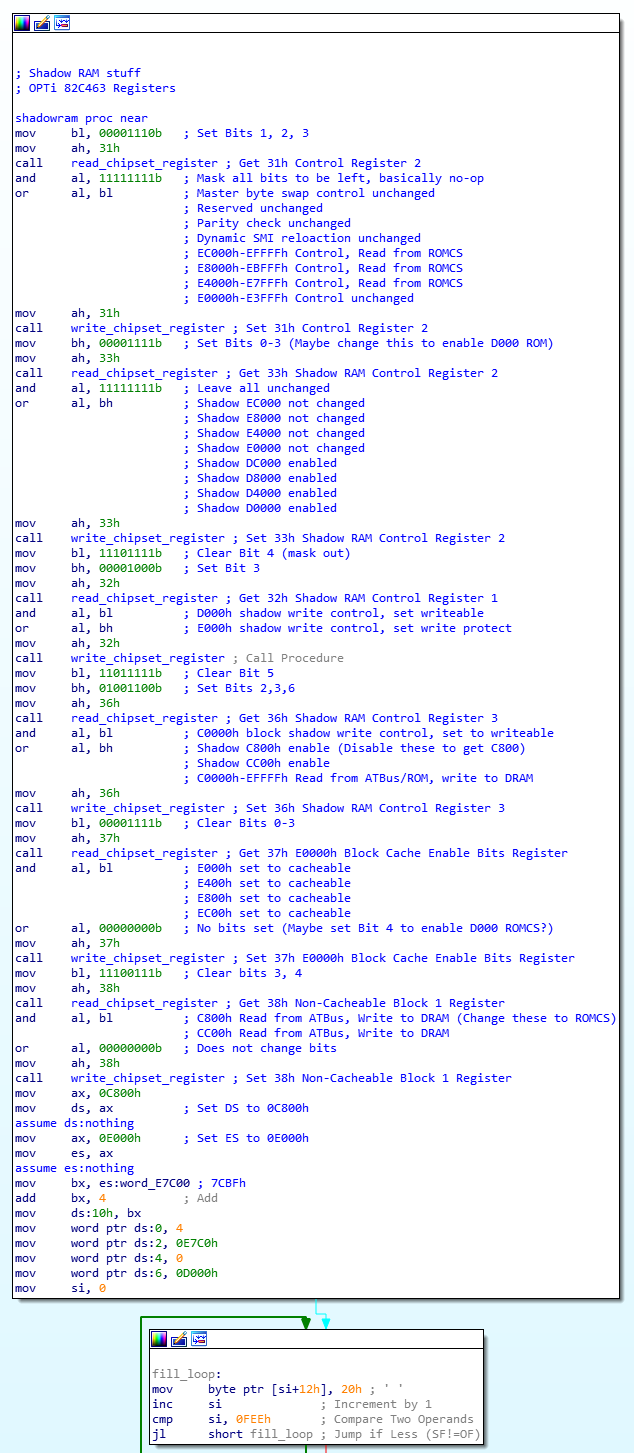
Then the sub function does some moving data around in a convoluted loops, that I have not bother to decipher further:
shadowram2.PNG

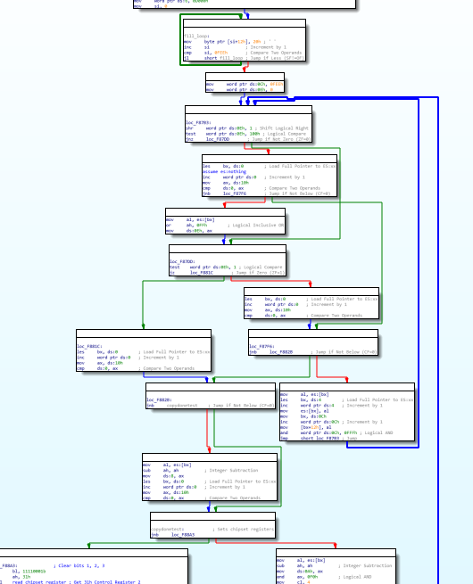
After that is complete, we get back to setting some registers:
shadowram3.PNG
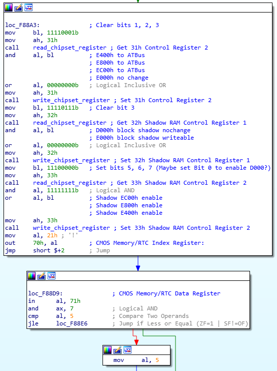
This time, it seems to be for the E000h segment, which contains the power management BIOS and possibly the BIOS setup (which, by the way, can be accessed anytime with the FN+F4 key, even on DOS).

Next, the function performs copying and checksumming:
shadowram4.PNG

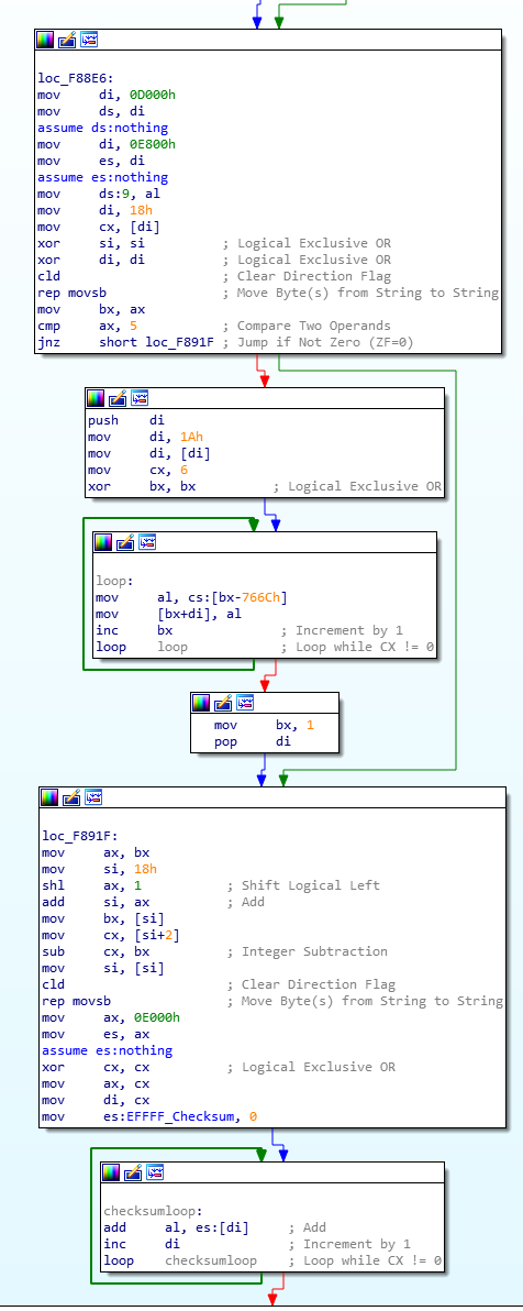
Finally, we reach the end of the function:
shadowram5.PNG
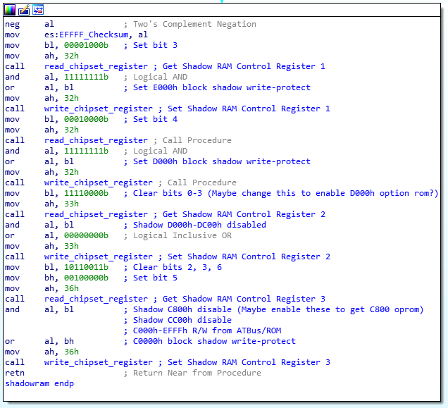
At the end, the shadow RAM segments are either enabled or disabled depending on whether they are used for ROM data, and they are also set to write-protected.

I have looked over the shadow ram function over and over, and with datasheet for the 82C463, deduced what register values possibly need to be changed to enable either the C800h or D000h segment decoding and shadowing.
C800h segment would be problematic for the XTIDE Universal BIOS, because the C800h-CFFFh area is used also for the PCMCIA, and I do want to use ATA card, that at least by default maps to C800h and C900h. Maybe that can be changed
just by giving the PCMCIA card services software different addresses in the config.sys and also excluding that from emm386, but D000h would be better for the XTIDE bios.

I have ended up testing couple different configurations:
For D000h: XTIDE Bios to 10000h in the dump file
38717: B7 0F -> 0E Set "32h Shadow D0000-D3FFF" Disabled (at the beginning of the shadowram.asm)
38754: C3 00 -> 10 Set "37h D0000 ROMCS#"
38972: B3 F0 -> F1 Set "32h Shadow D0000-D3FFF" Enabled(at the end of the shadowram.asm)

For C800: Place XTIDE Bios to 8000h in the dump file
3EBB0: 86 -> 9E Enable C800,CC00 ROMCS# (In the initial chipset register table)
3873A : B7 4C -> B7 40 C800,CC00 Shadow disable (at the beginning of the shadowram.asm)
3875A : B3 E7 -> B3 FF C800,CC00 to ROMCS#
38981: B3 B3 -> B3 BF Shadow C800,CC00 Enable (at the end of the shadowram.asm)

I have configured the XTIDE ide_386l.bin with the XTIDECFG.COM run on the Echos 44, and it correctly found 1 16-bit ata controller. I assume, Olivetti used the standard I/O ports for the controller, at least that is what the config utility set those.
Then I inserted the XTIDE bios to the dump, either in the C800h segment or in the D000h segment,
and patched the system bios to use above register values to (maybe) enable the rom decoding and shadow ram.
Then I just flashed the eeprom back to the chip, and tested it on the Echos 44.

So far, the results have been mixed. In both configurations, I need to press Ctrl+Alt+Del after the Fixed Disk and Floppy Drives post-test, or else the system hangs at that point.
After the soft reboot, I get message: "Option ROM at C800:000 Pass" or "Option ROM at D000:000 Pass" depending which patch I flashed to the bios.

But, but...
If the CF card is in the system, it just hangs after the Option ROM message. But if I remove the CF card, then start system, soft reboot it,
XTIDE bios starts and shows the menu screen. I then can boot from the floppy drive in the XTIDE menu, and OS loads just fine.
Also, I can't enter into the system bios setup menu, when the option rom is enabled.

It seems that there might still be something wrong with the chipset register configuration and possibly with the XTIDE configuration as well. At this point, I'm a bit stuck and have decided to make this post public, in the hopes that someone else may have some insight or experience in enabling Option ROM regions in an embedded BIOS ROM.

Attachments

Reply 1 of 4, by jakethompson1

User metadata
Rank Oldbie
Rank
Oldbie

Dump the XT-IDE ROM from D000: after you've booted into DOS, and make sure it's an exact match with your ide_386l.bin?
also: there's a utility out there, I can't remember its name, to make a boot disk that loads an option ROM like XT-IDE into RAM and boots it, so that you can test and make sure it isn't an XT-IDE problem.

Reply 2 of 4, by Ketturi

User metadata
Rank Newbie
Rank
Newbie

I managed to get the XTIDE bios to boot and find the hard drive. It seems like problem is in the chipset registers and shadow ram configuration. Possibly because at that point system bios is trying to call the setup menu from the E800:0 and if that fails system just hangs.

Reply 3 of 4, by Ketturi

User metadata
Rank Newbie
Rank
Newbie

After looking deeper into the disassembled bios, it seems that the subfunction on the first post does not do general shadow copy. It is just for the setup menu, that resides in the "hidden" memory, and is probably executed through a protected mode paging. I found parts that do the actual shadow copy and register settings for the video bios, extended bios and system bios.

This is function for the video bios:

vbiosshadow     proc near               ; CODE XREF: runvbiosshadow+D↑p
pushf ; Push Flags Register onto the Stack
cli ; Clear Interrupt Flag
mov bl, 11111001b
mov ah, i38h_NCB1
call read_chipset_register ; 38h Non-Cacheable Block 1 Register

and al, bl ; C4000h R/W from AT-Bus
; C0000h R/W from AT-Bus
or al, 00000000b ; Logical Inclusive OR
mov ah, i38h_NCB1
call write_chipset_register ; 38h Non-Cacheable Block 1 Register

mov bl, 11011111b
mov ah, i36h_ShadowRAM_3
call read_chipset_register ; 36h Shadow RAM Control Register III

and al, bl ; C0000h-EFFFFh R/W from AT-Bus or ROMCS#
or al, 00000000b ; Logical Inclusive OR
mov ah, i36h_ShadowRAM_3
call write_chipset_register ; 36h Shadow RAM Control Register III

mov bl, 00000011b
mov ah, i36h_ShadowRAM_3
call read_chipset_register ; 36h Shadow RAM Control Register III

and al, 11111111b ; Logical AND
or al, bl ; Shadow C0000-C3FFFh enable
; Shadow C4000-C7FFFh enable
mov ah, i36h_ShadowRAM_3
call write_chipset_register ; 36h Shadow RAM Control Register III

mov cx, 4000h
mov ax, 0C000h
mov es, ax
assume es:nothing
call fill_AA55 ; Fills segment starting from ES, CX bytes long, with AA55 id

mov cx, 4000h
call test_AA55 ; Checks area starting from ES, CX long, if it is full of AA55 id

jnb short doshadowC ; Jump if Not Below (CF=0)

mov bl, 00000110b
mov ah, i38h_NCB1
call read_chipset_register ; 38h Non-Cacheable Block 1 Register

and al, 11111111b ; Logical AND
or al, bl ; C4000h-C7FFFh R/W from ROMCS#
; C0000h-C3FFFh R/W from ROMCS#
mov ah, i38h_NCB1
call write_chipset_register ; 38h Non-Cacheable Block 1 Register

mov bl, 10111111b
mov ah, i36h_ShadowRAM_3
call read_chipset_register ; 36h Shadow RAM Control Register III

and al, bl ; C0000h-EFFFFh R/W from AT-Bus/ROMCS#
or al, 00000000b ; Logical Inclusive OR
mov ah, i36h_ShadowRAM_3
Show last 118 lines
                call    write_chipset_register ; 36h Shadow RAM Control Register III

mov bl, 11111100b
mov ah, i36h_ShadowRAM_3
call read_chipset_register ; 36h Shadow RAM Control Register III

and al, bl ; Shadow C4000h-C7FFFh disable
; Shadow C0000h-C3FFFh disable
or al, 00000000b ; Logical Inclusive OR
mov ah, i36h_ShadowRAM_3
call write_chipset_register ; 36h Shadow RAM Control Register III

jmp shadowcopyfailed ; Jump

; ---------------------------------------------------------------------------

doshadowC: ; CODE XREF: vbiosshadow+43↑j
mov bl, 11111100b
mov ah, i36h_ShadowRAM_3
call read_chipset_register ; 36h Shadow RAM Control Register III

and al, bl ; Shadow C4000h-C7FFFh disable
; Shadow C0000h-C3FFFh disable
or al, 00000000b ; Logical Inclusive OR
mov ah, i36h_ShadowRAM_3
call write_chipset_register ; 36h Shadow RAM Control Register III

mov bl, 00000110b
mov ah, i38h_NCB1
call read_chipset_register ; 38h Non-Cacheable Block 1 Register

and al, 11111111b ; Logical AND
or al, bl ; C4000h-C7FFFh R/W from ROMCS#
; C0000h-C3FFFh R/W from ROMCS#
mov ah, i38h_NCB1
call write_chipset_register ; 38h Non-Cacheable Block 1 Register

mov bl, 01000000b
mov ah, i36h_ShadowRAM_3
call read_chipset_register ; 36h Shadow RAM Control Register III

and al, 11111111b ; Logical AND
or al, bl ; C0000h-EFFFFh Read from AT/ROMCS, write to DRAM
mov ah, i36h_ShadowRAM_3
call write_chipset_register ; 36h Shadow RAM Control Register III

mov ax, 0C000h ; Start from C000
mov ds, ax
assume ds:nothing
mov es, ax
xor si, si ; Logical Exclusive OR
xor di, di ; Logical Exclusive OR
mov cx, 4000h ; Copy 16k
cld ; Clear Direction Flag
rep movsw ; Move Byte(s) from String to String
mov bl, 00100000b
mov ah, i36h_ShadowRAM_3
call read_chipset_register ; 36h Shadow RAM Control Register III

and al, 11111111b ; Logical AND
or al, bl ; C0000h block write protect
mov ah, i36h_ShadowRAM_3
call write_chipset_register ; 36h Shadow RAM Control Register III

mov bl, 00000011b
mov ah, i36h_ShadowRAM_3
call read_chipset_register ; 36h Shadow RAM Control Register III

and al, 11111111b ; Logical AND
or al, bl ; Shadow C4000h-C7FFFh enable
; Shadow C0000h-C3FFFh enable
mov ah, i36h_ShadowRAM_3
call write_chipset_register ; 36h Shadow RAM Control Register III

mov bl, 11111001b
mov ah, i38h_NCB1
call read_chipset_register ; 38h Non-Cacheable Block 1 Register

and al, bl ; C4000h-C7FFFh R/W from AT-Bus
; C0000h-C3FFFh R/W from AT-Bus
or al, 00000000b ; Logical Inclusive OR
mov ah, i38h_NCB1
call write_chipset_register ; 38h Non-Cacheable Block 1 Register

mov bl, 00011000b
mov ah, i38h_NCB1
call read_chipset_register ; 38h Non-Cacheable Block 1 Register

and al, 11111111b ; Logical AND
or al, bl ; CC000h-CFFFFh R/W from ROMCS#
; C8000h-CBFFFh R/W from ROMCS#
mov ah, i38h_NCB1
call write_chipset_register ; 38h Non-Cacheable Block 1 Register

mov al, 0E4h
call readcmosreg ; AL: Index of CMOS Register
; Returns data from CMOS in AH

or ah, 2 ; Logical Inclusive OR
dec al ; Decrement by 1
call writecmosreg ; AL: Index of CMOS
; AH: Data to be writen into CMOS register

popf ; Pop Stack into Flags Register
clc ; Clear Carry Flag
jmp short return ; Jump

; ---------------------------------------------------------------------------

shadowcopyfailed: ; CODE XREF: vbiosshadow+75↑j
popf ; Pop Stack into Flags Register
stc ; Set Carry Flag


return: ; CODE XREF: vbiosshadow+108↑j
retn ; Return Near from Procedure

vbiosshadow endp

And this is function for the system bios:

f000shadow      proc near               ; DATA XREF: copyf000shadow+D↑o
mov bl, 10000000b
mov ah, i32h_ShadowRAM_1
call read_chipset_register ; Call Procedure

and al, 11111111b ; Logical AND
or al, bl ; F000-FFFF Read from ROMCS#
mov ah, i32h_ShadowRAM_1
call write_chipset_register ; Call Procedure

mov bl, 01111111b
mov ah, i36h_ShadowRAM_3
call read_chipset_register ; Call Procedure

and al, bl ; F000 block write to DRAM
or al, 00000000b ; Logical Inclusive OR
mov ah, i36h_ShadowRAM_3
call write_chipset_register ; Call Procedure

mov cx, 8000h ; Fill 32k
mov ax, 0F000h ; Start from F000
mov es, ax
assume es:seg005
call fill_AA55 ; Fills segment starting from ES, CX bytes long, with AA55 id

mov bl, 01111111b
mov ah, i32h_ShadowRAM_1
call read_chipset_register ; Call Procedure

and al, bl ; F000-FFFF Read rom DRAM
or al, 0 ; Logical Inclusive OR
mov ah, i32h_ShadowRAM_1
call write_chipset_register ; Call Procedure

mov cx, 8000h
call test_AA55 ; Checks area starting from ES, CX long, if it is full of AA55 id

jnb short doshadowF ; Jump if Not Below (CF=0)

mov bl, 10000000b
mov ah, i32h_ShadowRAM_1
call read_chipset_register ; Call Procedure

and al, 11111111b ; Logical AND
or al, bl ; F000-FFFF Read from ROMCS#
mov ah, i32h_ShadowRAM_1
call write_chipset_register ; Call Procedure

mov bl, 10000000b
mov ah, i36h_ShadowRAM_3
call read_chipset_register ; Call Procedure

and al, 11111111b ; Logical AND
or al, bl ; F000-FFFF write to ROMCS#
mov ah, i36h_ShadowRAM_3
call write_chipset_register ; Call Procedure

jmp shadowcopyfailed ; Jump

; ---------------------------------------------------------------------------
Show last 263 lines

doshadowF: ; CODE XREF: f000shadow+41↑j
mov bl, 10000000b
mov ah, i32h_ShadowRAM_1
call read_chipset_register ; Call Procedure

and al, 11111111b ; Logical AND
or al, bl ; F000-FFFF Read from ROMCS#
mov ah, i32h_ShadowRAM_1
call write_chipset_register ; Call Procedure

mov ax, 0F000h ; Start copy from F000
mov ds, ax
mov es, ax
xor si, si ; Logical Exclusive OR
xor di, di ; Logical Exclusive OR
mov cx, 8000h ; Copy 32k
cld ; Clear Direction Flag
rep movsw ; Move Byte(s) from String to String
mov bl, 01111111b
mov ah, i32h_ShadowRAM_1
call read_chipset_register ; Call Procedure

and al, bl ; F000-FFFF Read from DRAM
or al, 00000000b ; Logical Inclusive OR
mov ah, i32h_ShadowRAM_1
call write_chipset_register ; Call Procedure

jmp short testE000 ; Jump

; ---------------------------------------------------------------------------

testentry:
test bh, 2 ; Logical Compare
jnz short testE000 ; Jump if Not Zero (ZF=0)

mov bl, 00001111b
mov ah, i31h_Control_2
call read_chipset_register ; Call Procedure

and al, 11111111b ; Logical AND
or al, bl ; E000-EFFF R/W from ROMCS#
mov ah, i31h_Control_2
call write_chipset_register ; Call Procedure

mov bl, 10111111b
mov ah, i36h_ShadowRAM_3
call read_chipset_register ; Call Procedure

and al, bl ; C000-EFFF R/W from AT-Bus/ROMCS#
or al, 00000000b ; Logical Inclusive OR
mov ah, i36h_ShadowRAM_3
call write_chipset_register ; Call Procedure

mov bl, 00001111b
mov ah, i33h_ShadowRAM_2
call read_chipset_register ; Call Procedure

and al, bl ; Logical AND
or al, 00000000b ; Logical Inclusive OR
mov ah, i33h_ShadowRAM_2
call write_chipset_register ; Call Procedure

jmp shadowok ; Jump

; ---------------------------------------------------------------------------

testE000: ; CODE XREF: f000shadow+97↑j
; f000shadow+9C↑j
mov bl, 11110000b
mov ah, i31h_Control_2
call read_chipset_register ; Call Procedure

and al, bl ; E000-EFFF R/W from AT-Bus
or al, 00000000b ; Logical Inclusive OR
mov ah, i31h_Control_2
call write_chipset_register ; Call Procedure

mov bl, 11110000b
mov ah, i33h_ShadowRAM_2
call read_chipset_register ; Call Procedure

and al, 11111111b ; Logical AND
or al, bl ; Shadow E000-EFFF enable
mov ah, i33h_ShadowRAM_2
call write_chipset_register ; Call Procedure

mov bl, 00000010b
mov ah, i35h_DRAM_2
call read_chipset_register ; Call Procedure

and al, 11111111b ; Logical AND
or al, bl ; Set all DRAM not cacheable
mov ah, i35h_DRAM_2
call write_chipset_register ; Call Procedure

mov bl, 00001111b
mov ah, i37h_E000h_cache
call read_chipset_register ; Call Procedure

and al, 11111111b ; Logical AND
or al, bl ; Set E000-EFFF cacheable
mov ah, i37h_E000h_cache
call write_chipset_register ; Call Procedure

mov bl, 11110111b
mov ah, i32h_ShadowRAM_1
call read_chipset_register ; Call Procedure

and al, bl ; Set E000 block shadow writeable
or al, 00000000b ; Logical Inclusive OR
mov ah, i32h_ShadowRAM_1
call write_chipset_register ; Call Procedure

mov cx, 8000h ; Fill 32k
mov ax, 0E000h ; Start from E000h
mov es, ax
assume es:nothing
call fill_AA55 ; Fills segment starting from ES, CX bytes long, with AA55 id

mov cx, 8000h
call test_AA55 ; Checks area starting from ES, CX long, if it is full of AA55 id

jnb short doshadowE ; Jump if Not Below (CF=0)

mov bl, 00001111b
mov ah, i31h_Control_2
call read_chipset_register ; Call Procedure

and al, 11111111b ; Logical AND
or al, bl ; E000-EFFF R/W from ROMCS#
mov ah, i31h_Control_2
call write_chipset_register ; Call Procedure

mov bl, 10111111b
mov ah, i36h_ShadowRAM_3
call read_chipset_register ; Call Procedure

and al, bl ; C000-EFFFh R/W from AT-Bus/ROMCS#
or al, 00000000b ; Logical Inclusive OR
mov ah, i36h_ShadowRAM_3
call write_chipset_register ; Call Procedure

mov bl, 00001111b
mov ah, i33h_ShadowRAM_2
call read_chipset_register ; Call Procedure

and al, bl ; Shadow E000-EFFF disable
or al, 00000000b ; Logical Inclusive OR
mov ah, i33h_ShadowRAM_2
call write_chipset_register ; Call Procedure

jmp shadowcopyfailed ; Jump

; ---------------------------------------------------------------------------

doshadowE: ; CODE XREF: f000shadow+132↑j
mov bl, 00001111b
mov ah, i33h_ShadowRAM_2
call read_chipset_register ; Call Procedure

and al, bl ; Shadow E000-EFFF disable
or al, 00000000b ; Logical Inclusive OR
mov ah, i33h_ShadowRAM_2
call write_chipset_register ; Call Procedure

mov bl, 00001111b
mov ah, i31h_Control_2
call read_chipset_register ; Call Procedure

and al, 11111111b ; Logical AND
or al, bl ; E000-EFFF Read from ROMCS#
mov ah, i31h_Control_2
call write_chipset_register ; Call Procedure

mov bl, 01000000b
mov ah, i36h_ShadowRAM_3
call read_chipset_register ; Call Procedure

and al, 11111111b ; Logical AND
or al, bl ; C000-EFFF Read from AT-Bus/ROMCS#, write to DRAM
mov ah, i36h_ShadowRAM_3
call write_chipset_register ; Call Procedure

mov ax, 0E000h ; Start from E000
mov ds, ax
assume ds:nothing
mov es, ax
xor si, si ; Logical Exclusive OR
xor di, di ; Logical Exclusive OR
mov cx, 8000h ; Copy 32k
cld ; Clear Direction Flag
rep movsw ; Move Byte(s) from String to String
mov bl, 00001000b
mov ah, i32h_ShadowRAM_1
call read_chipset_register ; Call Procedure

and al, 11111111b ; Logical AND
or al, bl ; Set E000 block shadow write protected
mov ah, i32h_ShadowRAM_1
call write_chipset_register ; Call Procedure

mov bl, 11110000b
mov ah, i33h_ShadowRAM_2
call read_chipset_register ; Call Procedure

and al, 11111111b ; Logical AND
or al, bl ; Shadow E000-EFFF enable
mov ah, i33h_ShadowRAM_2
call write_chipset_register ; Call Procedure

mov bl, 11110000b
mov ah, i31h_Control_2
call read_chipset_register ; Call Procedure

and al, bl ; E000-EFFF R/W from AT-Bus
or al, 00000000b ; Logical Inclusive OR
mov ah, i31h_Control_2
call write_chipset_register ; Call Procedure


shadowok: ; CODE XREF: f000shadow+CE↑j
jmp short $+2 ; Jump

; ---------------------------------------------------------------------------

invalidatecache: ; CODE XREF: f000shadow:shadowok↑j
invd ; Invalidate Data Cache
jmp far ptr shadowenabled ; Jump

; ---------------------------------------------------------------------------

shadowenabled: ; CODE XREF: f000shadow+1DC↑J
mov al, 0E4h
mov ah, 1
call writecmosreg ; AL: Index of CMOS
; AH: Data to be writen into CMOS register

popf ; Pop Stack into Flags Register
clc ; Clear Carry Flag
jmp short return ; Jump

; ---------------------------------------------------------------------------
db 90h
; ---------------------------------------------------------------------------

shadowcopyfailed: ; CODE XREF: f000shadow+63↑j
; f000shadow+164↑j
jmp far ptr noshadow ; Jump

; ---------------------------------------------------------------------------

noshadow: ; CODE XREF: f000shadow:shadowcopyfailed↑J
popf ; Pop Stack into Flags Register
stc ; Set Carry Flag


return: ; CODE XREF: f000shadow+1EA↑j
retn ; Return Near from Procedure

f000shadow endp

I could not find watertight entry points for these functions, but at least for the system bios shadow procedure, the function is first copied into the ram, and then executed there not to interfere with the process.

From these functions I deduced these register values for the chipset to enable the option rom areas:

To shadow D000:

33h:0 0 D000 Shadow disable
37h:4 1 D000 Read from ROMCS# (31h for E000)
36h:6 1 C000-EFFF Read from AT-Bus/ROMCS#, write to DRAM
Do a copy to D000
32h:4 1 D000 block write protected
33h:0 1 D000 Shadow enabled
37h:4 0 D000 R/W from AT-Bus (31h for E000)

To not shadow D000:

37h:4 1	 D000 R/W from ROMCS#
36h:6 0 C000-EFFF R/W from AT-Bus/ROMCS#
33h:0 0 D000 Shadow disable

To shadow C800:

36h:2-3	0  C800-CFFF Shadow disable
38h:3-4 1 C800-CFFF R/W from ROMCS#
36h:6 1 C000-EFFF Read from AT-Bus/ROMCS#, write to DRAM
Do a copy to C800
36h:5 1 C000 block write protect
36h:2-3 1 C800-CFFF shadow enabled
38h:3-4 0 C800-CFFF R/W from AT-Bus

To not shadow C800:

38h:3-4	1 C800-CFFF R/W from ROMCS#
36h:6 0 0 C000-EFFF R/W From AT-BUS/ROMCS#
36h:2-3 0 C800-CFFF Shadow disable

I just need to find place to set these registers and do the copy. It could be possible to use the system bios shadow copy procedure, and just give it last segment of the D000 block, and increase the CX register value where the copy is done.

The Olivetti BIOS is very convoluted, and IDA does not follow it properly, so it has been bit difficult to do the reverse-engineering. At the begining when the ram is not yet initialized, there is no call instruction available, and instead SP and return is used to do the jumps. This confuses heck out of the IDA. Also parts of the code is then copied to the ram, and executed there. I also found 3 different places, where the different chipset register table is loaded into the chipset. At least two of them touch the register I am interested in. The resume and standby functionality does not help either, as these are handled differently by the BIOS boot process, and part of the normal POST is skipped.

Reply 4 of 4, by Ketturi

User metadata
Rank Newbie
Rank
Newbie

It seems like I finally got the XTIDE Bios to work properly. I had to place the XTIDE bios to the CC00 segment, because for the life I could not get the D000-DFFF segments to show up as a rom, even though all registers were properly configured. I think there is some protected mode and memory paging magic going round. CC00 segment should be ok in theory, as the PCMCIA controller can be configured to map the memory windows to different segments. The system bios by default sets the memory windows of PCMCIA to C800-CA00 when the PCMCIA boot option is set enabled (It allows to boot from Linear SRAM/Flash cards as a floppy).

Here are the modifications I had to do to the bios:

Enable XTIDE universal bios in CC00-CFFF 16k ROM block:

VideoShadow at A4AD:
RAM test: (Actually, do not modify, C800 could cause overwrite on pcmcia?
FA4AF: B3 F9 -> ;38h CC00h R/W from AT-Bus
FA4CF: B3 03 -> ;36h CC00h shadow enable
FA4DF: B9 00 40 -> B9 00 80 ;Fill 64k block instead of 32k.
FA4EA: B9 00 40 -> B9 00 80 ;Test 64k block instead of 32k

Disable shadow:
FA4F2: B3 06 -> B3 16 ;38h CC00h R/W from ROMCS#
FA512: B3 FC -> B3 F4 ;36h CC00h Shadow disable

Copy and enable shadow
FA525: B3 FC ->B3 F4 ;36h CC00h Shadow disable
FA535: B3 06 ->B3 16 ;38h CC00h R/W from ROMCS#
FA560: B9 00 40 -> B9 00 80 ;Copy 64k instead of 32k
FA576: B3 03 ->B3 0B ;36h CC00h Shadow enable
FA586: B3 F9 ->B3 E9 ;38h CC00h R/W from AT-Bus
FA596: B3 18 ->B3 08 ;38h CC00h R/W from ROMCS# mask out

C000Shadow at 3748:
F3748: B6 06 -> B6 16 ;38h CC00h R/W from ROMCS#
F3783: B9 00 40 -> B9 00 80, mov cx, 8000h ;Increase copy couunt from 32k to 64k block (C000-C7FF to C000-CFFF)
F3798: B3 03 -> B3 0B ;36h CC00h Shadow enable
F37A8: B3 F9 -> B3 E9 ;38h CC00h R/W from AT-Bus

E800Shadow at 8706:
F873A: B7 4C -> B7 44 ;36h CC00h Shadow mask out
F875A: B3 E7 -> B3 F7 ;38h CC00h R/W AT-Bus mask out
F8981: B3 B3 -> B3 BB ;38h CC00h Shadow mask out

ChipsetInit:
FEBB0: 86 -> 96
F8349: 86 -> 96

Checksum:
FFFFF: 32 -> 92

I included the patched bios as attachment. With these mods, XTIDE loads up properly, and is working shadow and cache memory enabled or disabled from the bios setup. Also the bios setup seems to work. I have not tested the suspend functionality yet, but at least warm boot with reduced post tests seem to work. Only issue remaining is that when the bios setup triggers reboot after changing values I need to do hard reset.

Attachments