majestyk wrote on 2023-10-11, 16:12:
Good work, I saved the diagrams for future use / reference!
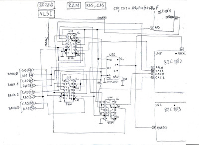
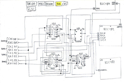
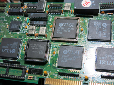
Thanks. Here are a couple more diagrams and pictures. I also added reverse engineering for another 286 motherboard which I called MB2. The schematic looks a bit different but the conception is completely the same.
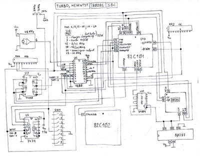
I’m already close to starting to transfer all this to KiCAD, I’ll see what happens with my free time. I have added a significantly updated and refined wait-state and turbo circuit scematic. I also noticed that the PAL16R6 uses only 3 output pins - ROMWTST, XTAL 2(2) and SYSCLK, and nothing more. All other pins 13-17 are not used anywhere. And despite the fact that pins 3-8 are connected to A0, A1, -S0, -S1, etc., they are not used anywhere as well on that chip. I still don’t understand why they had to be led to this PAL.
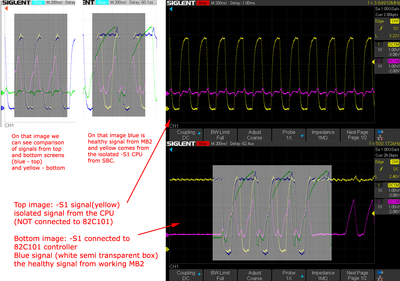
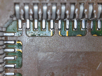
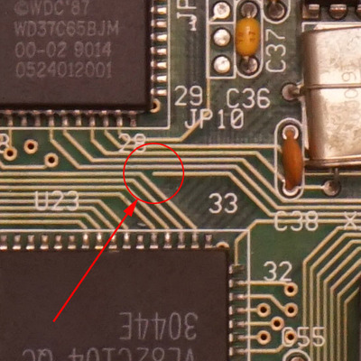
Further. I resoldered all VLSI chipset connectors and it didn't help. SBC still not working. But I found one strange thing. The screenshot is attached. I compared -S0, -S1, A0, and A1 with the working 286 motherboard (MB2) with this SBC and noticed that the signal looks almost normal, but something is missing. It seems that some chip is not receiving some signal. But I can’t figure out which one it is. I can’t understand how exactly the -S1 signal is generated. Accordingly, with datasheets, it's generated by the CPU. It is out of the CPU and going to 82C101, after which it receives full formation and here at this stage, something does not work as it should.
I can confidently say that I have carried out a complete reverse engineering of the main parts of the board and if desired, all this can be transferred to some kind of CAD and we will have another open-source project, but for 80286 based on VLSI.