VOGONS


First post, by numeriK

User metadata
Rank Newbie
Rank
Newbie

Hello everyone, I'm new to VOGONS, but not to "old tech". I grew up with 486's and had the opportunity recently to jump on some old hardware.

Among what I've picked up is a PC Chips M919 v1.5 with what appears to be 1024K cache in each bank (please confirm my suspicions). I booted the motherboard but didn't have an "AT-style" keyboard so I'm unable to do much at this point in time.

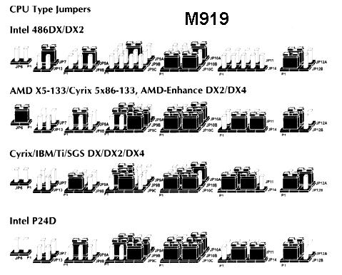
More importantly, does anyone know what the plethora of jumpers are for? It seems like there's ~15 more jumpers on this board than the v3.x series, and all I can find online are the spec sheets for the 3.x (doesn't really help me).

Please see the attached pictures, and thanks in advance!

Attachments

  • Filename
    M919CacheBanks.jpg
    File size
    109.07 KiB
    Downloads
    181 downloads
    File license
    Fair use/fair dealing exception
  • Filename
    M919Jumpers.jpg
    File size
    77.46 KiB
    Downloads
    166 downloads
    File license
    Fair use/fair dealing exception

8433UUD v2 | AMD 5x86 @ 180MHz (60MHz x 3, 30MHz PCI) | 64MB EDO | TNT 16MB PCI | SB AWE64 ISA | Win98SE

Reply 1 of 25, by feipoa

User metadata
Rank l33t++
Rank
l33t++

I see 256 KB of cache installed. The DIPs are of appropriate size if you have 1024 KB to plunk in there.

I wasn't aware the jumper layouts were much different aside from the cache jumpers. I have not used a v1.x before, so you may need to piece together jumpers positions from info that is silk screened on the PCB and from,
http://motherboards.mbarron.net/models/486pci/m919v1.htm

Plan your life wisely, you'll be dead before you know it.

Reply 3 of 25, by sliderider

User metadata
Rank l33t++
Rank
l33t++

You have to be sure that you actually have real cache chips and that the sockets are connected up. The PCCHIPS M919 was infamous for having fake cache installed and the BIOS hacked to show the presence of cache at start up even though there wasn't any.

At least your UMC chipset seems real. PCCHIPS was also infamous for using a generic chipset with stick on labels on top to make it look like a name brand chipset was being used.

Reply 4 of 25, by numeriK

User metadata
Rank Newbie
Rank
Newbie

I see 256 KB of cache installed. The DIPs are of appropriate size if you have 1024 KB to plunk in there.

Thanks feipoa, so basically - even though I have 4x2 banks of 256K chips, the TAG chip is all that really matters? So I could theroretically put a 512K or 1028K TAG chip in there to bump it up? I'm rusty on the "old tech" stuff, but it's slowly coming back to me!

I wasn't aware the jumper layouts were much different aside from the cache jumpers. I have not used a v1.x before, so you may need to piece together jumpers positions from info that is silk screened on the PCB and from,
http://motherboards.mbarron.net/models/...m919v1.htm

Many thanks! I actually found that already, but ironically it has the layout and jumper positions for a v3.x board - even though it says it's for v1.x... I'm sure that with some trial-and-error I'll be able to figure out most jumpers.

Are the DIP sockets even connected to anything?

Tracing some out on the underside of the board they lead to the UM8881F and the Socket3. I didn't trace them all, but it looks legit. After I get this thing running I'll be able to test and confirm if the cache even works - if it does I'll then consider bumping it up.

8433UUD v2 | AMD 5x86 @ 180MHz (60MHz x 3, 30MHz PCI) | 64MB EDO | TNT 16MB PCI | SB AWE64 ISA | Win98SE

Reply 5 of 25, by numeriK

User metadata
Rank Newbie
Rank
Newbie

You have to be sure that you actually have real cache chips and that the sockets are connected up. The PCCHIPS M919 was infamous for having fake cache installed and the BIOS hacked to show the presence of cache at start up even though there wasn't any.

Yeah, that's what I'm hearing as I float around VOGONS and the web regarding this board. I'll be able to confirm within the coming days.

8433UUD v2 | AMD 5x86 @ 180MHz (60MHz x 3, 30MHz PCI) | 64MB EDO | TNT 16MB PCI | SB AWE64 ISA | Win98SE

Reply 6 of 25, by RacoonRider

User metadata
Rank Oldbie
Rank
Oldbie
numeriK wrote:

Thanks feipoa, so basically - even though I have 4x2 banks of 256K chips, the TAG chip is all that really matters? So I could theroretically put a 512K or 1028K TAG chip in there to bump it up? I'm rusty on the "old tech" stuff, but it's slowly coming back to me!

Tag chip size does not matter in most cases. You have 8*256K chips. 8*256K/8=256KB

K is kilobit, KB is kilobyte, that's the trick.

Reply 7 of 25, by Anonymous Coward

User metadata
Rank l33t
Rank
l33t

The tag chip certainly does matter, though I am not sure what will happen if you use a tag that is too small. Certainly nothing bad will happen from having a tag chip that is too large though. Motherboard manuals are usually very specific about matching cache sizes with their corresponding tag rams.

"Will the highways on the internets become more few?" -Gee Dubya
V'Ger XT|Upgraded AT|Ultimate 386|Super VL/EISA 486|SMP VL/EISA Pentium

Reply 8 of 25, by numeriK

User metadata
Rank Newbie
Rank
Newbie

Tag chip size does not matter in most cases. You have 8*256K chips. 8*256K/8=256KB

K is kilobit, KB is kilobyte, that's the trick.

Ding! Ding! Ding! Well the light bulb just turned on because I knew I was not adding it up correctly.

Thanks for the clarification!

8433UUD v2 | AMD 5x86 @ 180MHz (60MHz x 3, 30MHz PCI) | 64MB EDO | TNT 16MB PCI | SB AWE64 ISA | Win98SE

Reply 9 of 25, by GXL750

User metadata
Rank Member
Rank
Member

With any PC Chips product from before 1997, just assume there's no L2 cache. Also don't bank on the thing being reliable. However, you can have some fun with the board. I remember the m919 having a lot of speed options and, without any l2 cache, the thing makes for a decent overclocking board.

Reply 11 of 25, by numeriK

User metadata
Rank Newbie
Rank
Newbie

Hi guys, I finally have a keyboard and I'm tinkering around with this thing. Every time I attempt any sort of stress test the machine freezes. I have a feeling the problem lies with these jumpers...

If you look at the bottom of this page,
http://th2chips.freeservers.com/m919/jumper/index.html

You'll see this image:
m919j2.gif

By the looks of that J6 should be closed for an AMD 5x86. The J6 on my v1.5 motherboard is a fan header next to the CPU socket. It's 4 pins and is silk screened as "J6 5V G G 12V". I put a multimeter to it and it's correct. I have a CPU fan running on it no problem.

In the image, next to J6, J7 and J13 should be open. Well J7 on my board is a set of 3 jumpers to set the bus speed (25, 33, 40, or 50MHz). How these 3 jumpers are open/closed determines that speed and it's silk screened on the board. J13 is the jumper for my Reset switch on the front panel.

As you can see, the pin out of the v3.x boards seem to be, quite literally, completely different.

If anyone has any information at all on the v1.x boards it would be GREATLY appreciated!

Thanks all!

8433UUD v2 | AMD 5x86 @ 180MHz (60MHz x 3, 30MHz PCI) | 64MB EDO | TNT 16MB PCI | SB AWE64 ISA | Win98SE

Reply 12 of 25, by numeriK

User metadata
Rank Newbie
Rank
Newbie

Update: I referenced the jumper settings in the pictures on this thread:
FS: PC Chips 486 mobo and Almost Everything Else needed to Put Together a 486

J33 was closed on mine, but open on his, so I opened it and it changed how my mobo see's the CPU (from a 5x86 133MHz to a DX4 100MHz). Now it seems to be running without issue (at the moment)...

More to come, I'm sure!

8433UUD v2 | AMD 5x86 @ 180MHz (60MHz x 3, 30MHz PCI) | 64MB EDO | TNT 16MB PCI | SB AWE64 ISA | Win98SE

Reply 13 of 25, by TELVM

User metadata
Rank Oldbie
Rank
Oldbie

Found this bit of info:

"Yup, "Write Back Cache On" is the patched fake BIOS message. If it had real L2 cache installed, it would report the actual amount of cache present, typically 256KB. I have a PC Chips M919 which has fake onboard cache but gives you a slot to install a proprietary SIMM-like stick containing 256K of real L2 cache. Later versions of the board don't have the fake chips installed, but you can still see the fake solder traces which go in circles and don't connect to anything else on the board!"

http://www.youtube.com/all_comments?v=wNpq0sybH6Q&page=1

Fake L2 in a PC Chips M509:

dscn3210i.jpg

dscn3211.jpg

dscn3212c.jpg

http://www.htforos.com/fruteria/tenia-que-ser … hips-t1088.html

Reply 14 of 25, by numeriK

User metadata
Rank Newbie
Rank
Newbie

So glad I don't have that version of the board! I'd be pissed if the chips came apart like that!

On a high note I've installed Windows 98SE w/ a TNT 16MB card, drivers and all.

I've also cranked up the voltages and successfully ran 3dbench and speedsys @ 50MHz FSB / 200MHz CPU.

However, booting into Windows I need to crank it down to 40MHz FSB / 160MHz CPU for stability.

Speedsys is *not* recognizing my DIP L2 cache, however my jumpers could be messed up, so I'm still investigating.

8433UUD v2 | AMD 5x86 @ 180MHz (60MHz x 3, 30MHz PCI) | 64MB EDO | TNT 16MB PCI | SB AWE64 ISA | Win98SE

Reply 15 of 25, by feipoa

User metadata
Rank l33t++
Rank
l33t++
numeriK wrote:

On a high note I've installed Windows 98SE w/ a TNT 16MB card, drivers and all.

Which driver version did you install? I haven't yet gotten to the mass of Win98 drivers I need to test out on a SiS-based 486 and the TNT. Part of the uncertainty of trying a bunch of drivers is that Windows 98 very often gets confused and leaves the yellow exclamation mark regardless of different driver versions.

Better yet, if you could zip up the Windows 98 drivers you used and attach them, I can install my TNT on an untainted UMC setup to verify TNT functionality. If that works, I'll try them on the SiS. If they are drivers which have already been linked elsewhere on this forum, could you direct me to the exact link?

What revision of the AMD X5 chip did you, briefly, get running at 200 MHz?

Plan your life wisely, you'll be dead before you know it.

Reply 16 of 25, by numeriK

User metadata
Rank Newbie
Rank
Newbie

Which driver version did you install? I haven't yet gotten to the mass of Win98 drivers I need to test out on a SiS-based 486 and the TNT. Part of the uncertainty of trying a bunch of drivers is that Windows 98 very often gets confused and leaves the yellow exclamation mark regardless of different driver versions.

Better yet, if you could zip up the Windows 98 drivers you used and attach them, I can install my TNT on an untainted UMC setup to verify TNT functionality. If that works, I'll try them on the SiS. If they are drivers which have already been linked elsewhere on this forum, could you direct me to the exact link?

I actually used Diamond's driver package, not nVidia's. I included it below, if you'd like to give it a shot (idk which TNT you have). With it I get no driver "issues" in Device Manager.

What revision of the AMD X5 chip did you, briefly, get running at 200 MHz?

Printed as follows:
Am5x86-133-P75
AMD-X5-ADW
A 9634 FPB

Attachments

  • Filename
    w9xv5555.exe
    File size
    4.04 MiB
    Downloads
    179 downloads
    File comment
    Diamond RIVA TNT Driver for Windows 95/98
    File license
    Fair use/fair dealing exception

8433UUD v2 | AMD 5x86 @ 180MHz (60MHz x 3, 30MHz PCI) | 64MB EDO | TNT 16MB PCI | SB AWE64 ISA | Win98SE

Reply 17 of 25, by feipoa

User metadata
Rank l33t++
Rank
l33t++

I have the Creative version of the card. I'm not sure if there is any limitation in using other vendor's drivers for the same GPU. It looks like your Diamond driver package is also found in that link posted by Swaaye previously, specifically at, ftp://84.205.160.1/drivers/vga/rivaTnT/diamond/550tnt/

I have deprioritised this project for the time being, but will pick it up again. Thanks for checking this.

Plan your life wisely, you'll be dead before you know it.

Reply 18 of 25, by numeriK

User metadata
Rank Newbie
Rank
Newbie

Well, silly me, I immediately put my timings on the cache @ 2-1-2 or 2-2-2... never relaxed it all the way to 3-2-3.

Guess what? 3-2-3 timings allows me to see the L2 cache @ 50-66MHz bus.

Time to rebenchmark everything with relaxed timings/L2 cache!

Anyone know where to find 10ns modules? I have 9x32-pin DIP sockets (1 for the TAG). 256k, 512k, or 1024k will work - the more the marrier!

8433UUD v2 | AMD 5x86 @ 180MHz (60MHz x 3, 30MHz PCI) | 64MB EDO | TNT 16MB PCI | SB AWE64 ISA | Win98SE

Reply 19 of 25, by numeriK

User metadata
Rank Newbie
Rank
Newbie

After further testing my previous assumption was incorrect.

What's actually Enabling and Disabling the L2 on this board is the BIOS option for "Normal" or "EDO" DRAM.

With "Normal" (FPM) the board sees no L2 cache. With "EDO" the board acknowledges L2 cache.

Can anyone with a M919 v1.x board confirm this? I thought initially it was the timings, but I later realised that I changed this option *and* the timings at the same time (woops). I later went back and changed it back to "Normal" and tada, no cache.

Strange PCChips boards!....... <sigh>

8433UUD v2 | AMD 5x86 @ 180MHz (60MHz x 3, 30MHz PCI) | 64MB EDO | TNT 16MB PCI | SB AWE64 ISA | Win98SE