Ah, here she is - the Pentium 60. 800nm manufacturing process, this chip is huge. S-Spec SX835so this is a C1 stepping with the FDIV bug.

Really a wonderful chip to photograph, and aside from a few bent pins it would probably, at least in the short term, still be a functional CPU if I put it in a compatible system (which sadly, I don't have). STill, I have some questions about this particular chip!
On a number of Intel processors there appears to be numbers in the corner of the cavity:

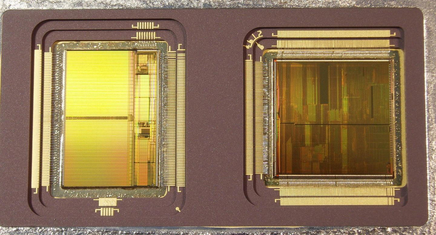
In this case, "4094". It's a code for something, but what? I might imagine that the "C" refers to the stepping. When you get into the actual silicon there are some weirdness too:

What's that diagonal line doing - some sort of shortcut? There's also this quizzical rectangle of two triangles - is that just filling in random space? Hunting around, we find even more worth questioning:

It looks like there's something on top of the die - an extra layer partially covering the diagonal red lines, but they are still visible below this odd covering. I wonder what the purpose is. And then you can't help but notice that super ominous triangle! What is it's purpose? Is it like a hidden Easter egg? Is it the way out of the maze if an electron was a maze runner?
Anyhow, this was a fun chip to photograph. Used three point light sources (flashlights) at different angles to get the full chip to be illuminated as you see it, while simultaneously firing a ring flash from the side to illuminate the chip cavity. The area beyond the cavity is artificially generated using the same texture as the ceramic to remove the solder and pins that would otherwise be on the chip.


