darrinh wrote on 2021-08-18, 22:12:
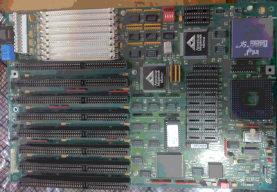
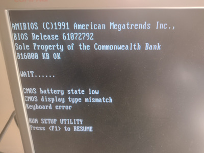
Thanks rmay635703 and mkarcher , I checked all the settings and installed memory and was able to power it on. The POST screen was very interesting however....
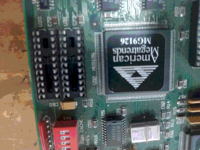
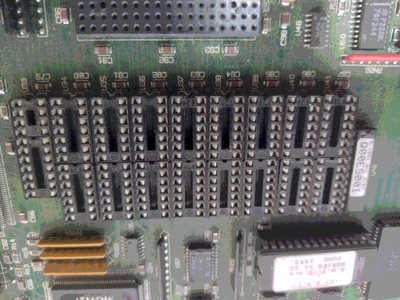
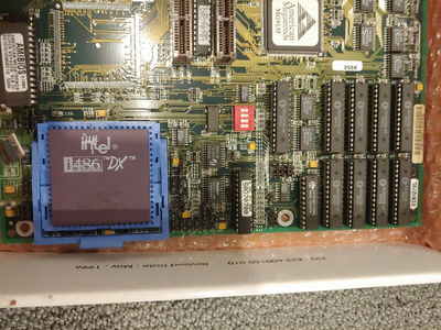
Frustratingly, I've not been able to find an image or information on what those missing chips are but U34-U41 are 28 pin sockets if I'm counting correctly and the board has a configuration switch that allows to switch between 64K and 256K (which ever is installed), so I guess they will be 28 pin srams ? U30/31 would be 32K x 8 22 pin ?
Oops, I did a mistake in my reasoning here. I've seen that U34-U41 are composed of two sockets. As narrow 28-pin sockets are much more available than 32-pin sockets (especially today, you don't get narrow 32-pin sockets at all), I supposed that U34-U41 were composed of 2*16 pin, not 2*14 pin. So U34-U41 are definitely meant to take 32K*8 chips for 256K cache or 8K*8 chips for 64K cache, providing either 16K or 4K of cache lines, 16 bytes each.
U30/31/33 are all 22-pin sockets, so I take all previous guesses back and claim that this is the very common classic old 386/486 cache chip layout: All three chips are 16K x 4. Two of them (U30/U31) are used in combination as 8 tag bits, and from U33 only a single bit is used as dirty indicator.
On later boards, usually the two 16K x 4 chips are replaced a by sinlge 32K x 8 chip (only using half of the chip, but 16K x 8 chips didn't exist back then). This happens especially with chipsets that can combine the dirty bit into the tag bits, or mainboards that use the cache just used in write-through mode, or run it in an "assume always dirty" configuration. In that case, the whole 256KB cache setup needs only a single kind of memory chips. Later on, memory manufacturers started producing 16K x 8 chips, with pinout identical to 32K x 8 chips, but ignoring one bit. Chips by Aster and Winbond did ignore a different bit, though. That's why some newer mainboards have a jumper to choose between "Aster tag" and "Winbond tag".