Reply 620 of 1228, by Sphere478

Rank
l33t++
- Rank
- l33t++
Doesn’t seem like much point in making that yellow cut as the motherboard and cpu internally will bridge across it
Doesn’t seem like much point in making that yellow cut as the motherboard and cpu internally will bridge across it
rasz_pl,
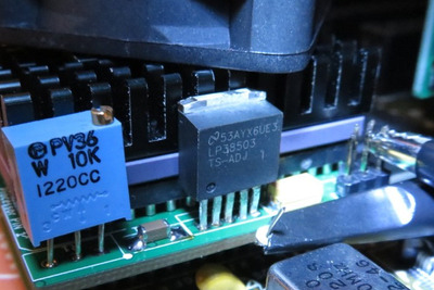
LP is a short abbreviation I'm using to distinguish between the two types of VRMs that I have and will work on this interposer. The LP38503TSX-ADJ is the currently installed VRM on the interposer.
Plan your life wisely, you'll be dead before you know it.
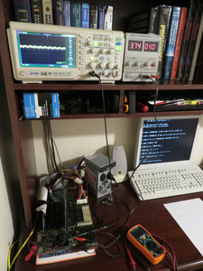
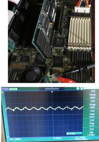
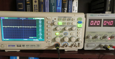
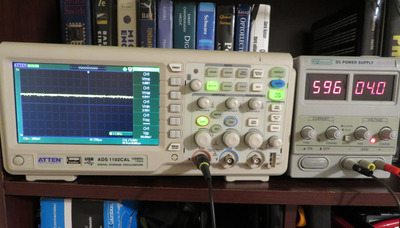
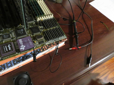
Due to the difficulty in constantly removing/resoldering the VRM, I'm doing these tests with my benchtop variable DC supply w/new cable. We can see the scope voltage reading and the supply reading are now in agreement.
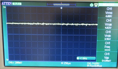
Here is the baseline for noise. On this motherboard, it is at 2.5 KHz rather than 800 Hz. The noise is still at 200 mV, with variances between 184 mV and 216 mV.
I remove the memory and turned the system on, but the noise is still present:
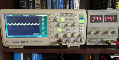
I did document some current measurements at 80 MHz,
3.6 V = 467 mA
3.8 V = 496 mA
4.0 V = 541 mA ---> becomes 600 mA at full load (DOOM)
4.2 V = 568 mA
4.4 V = 602 mA
4.6 V = 638 mA
4.7 V = 655 mA
4.8 V = 675 mA
4.9 V = 688 mA
5.0 V = 707 mA
At 40 MHz,
4.0 V = 374 mA
1 A seems like a realistic maximum, assuming 5.0 V at 100 MHz w/peltier.
Plan your life wisely, you'll be dead before you know it.
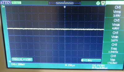
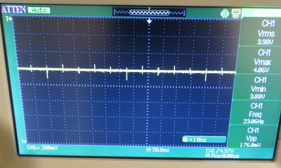
I figured out why the system was hanging with trying to clock-double on this motherboard. I was relying on the BIOS to setup the SXL parameters. I thought it had them correct, but I guess not, so I'm running them in software. I suspect caching of the adaptor ROM region was hanging the system. But here we can see after a hang-up, the noise and current draw drop.
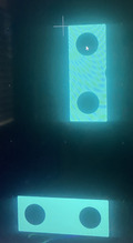
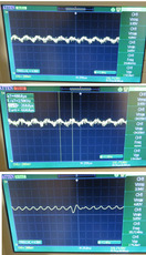
At 250 us (same as other scope images for low-freq):
And zoomed out to 50 ms:
And here we see the current drops to almost nil:
I'll get to work on adding those 100 nF ceramic caps to PGA pins.
Plan your life wisely, you'll be dead before you know it.
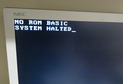
"System halted" screen finally made me realize bios is turning off interrupts and issuing HLT instruction = CPU is stopped.
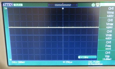
New_benchtop_setup_REMOVE_RAM_still_noise.JPG interesting, 2.5KHz still there, but high feq element is gone. CPU spinning executing loop from internal cache?
Would love to know where 2.5KHz (and 800Hz on another board) is coming from. Can you put another scope probe on HOLD/HLDA to see if there is any activity at all (and correlation)? Would stopping CPU for a brief moment produce such drastic ripple?
>The low frequency noise of 700 Hz varies somewhat depending on what crystal oscillator brand or speed is installed. I've seen 700 Hz, 800 Hz, or 1500 Hz.
could this really be harmonic from main oscillator? put another probe on CLK2 pin too see if thee is any correlation, but how?
all of the questions and no answers 😀
While I too would like to know the answer to the questions, their relevance will soon subside...
Plan your life wisely, you'll be dead before you know it.
Yes, I've seen oscillations at 700 Hz, 800 Hz, 1.5 KHz, and 2.5 KHz. I have dozens of different oscillators but I only tested a few. One yet another oscillator, there was no waveform but just noise over that 200 mV span.
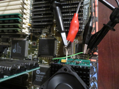
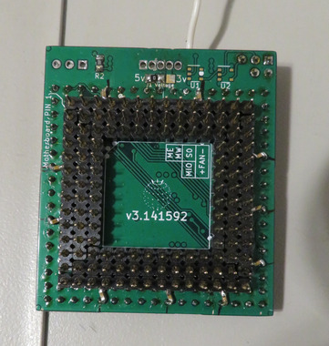
I have placed ten 100 nF 0805 capacitors in the configuration shown. I wasn't soldering for beauty here.

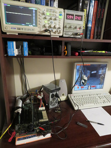
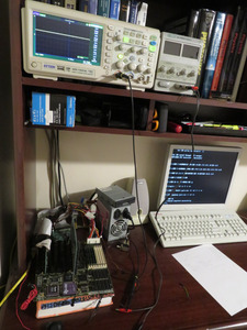
Here is the setup:
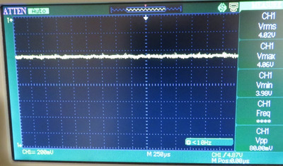
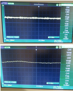
The oscillations disappeared and the noise is at 80 mV:
If I clock double, the noise reduces to around 64 mV:
This is a good deal improvement over the 200 mV (1x) and 160 mV (2x) noise witnessed without these 10 caps.
Plan your life wisely, you'll be dead before you know it.
If I leave the variable DC supply on, but turn off the motherboard, the noise is at around 16 mV:
An image showing the current used by the SXL2 at 80 MHz:
At this point, I'm wondering to myself: The motherboard only has two caps around the PGA132, so what kind of noise would we see if we install a regular ceramic SXL-40 PGA-132? The setup:
The noise was at 168 mV, but not really a waveform:
So perhaps the SXL2 interposer board is in resonance with whatever minor low frequency oscillation there is, thus amplifying it? Nonetheless, with an ordinary SXL showing 168 mV of noise, the SXL2 interposer without those ten 100 nF caps is probably within some tolerance. Obviously, I will be leaving the ten caps on my board. Their proximity to the PGA pins seems important since adding ceramic caps to the centre region did not help with the noise issue.
Next up, I will be removing all the centre caps and check for increased noise, if any, and optimise these values. Then will be adding the MIC branded VRM back onto the board, check noise, then swapping it for the LP branded VRM to compare the two VRMs. I will then assemble a second unit and try to determine if 10 caps are really necessary and if we can get away with just 4 PGA caps. Once this is determined, I bet we could add some 0603 sized solder pads next to these PGA pins. However, this may not be necessary
Plan your life wisely, you'll be dead before you know it.
However, this may not be necessary because if you haven't soldered the PGA on yet, you can fit an 0805 tightly between the pins, like so:
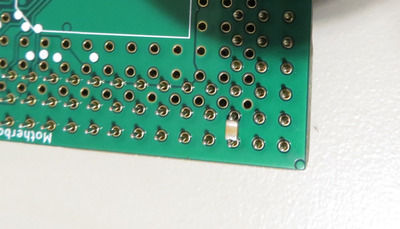
0603 is a bit harder to solder.
Plan your life wisely, you'll be dead before you know it.
feipoa wrote on 2022-12-05, 14:09:However, this may not be necessary because if you haven't soldered the PGA on yet, you can fit an 0805 tightly between the pins, like so:
IMG_1100.JPG0603 is a bit harder to solder.
that's actually fairly elegant, I like it
Sheesh, all I gotta do is add some silk there to indicate the cap. If those tiny caps between pins is all that is needed wonderful!
We are basically making a ppga pentium mmx 🤣
If you determine that the center region isn’t needed I can replace it with ground flood which will improve signal integrity
I can also try a different approach to how the center is configured
That is correct way to deal with! I said MLCC capacitors all along, But why is the 8 capacitors not populated in the center area, preferably large MLCC capacitors?
In newer designs and in all of the consoles including xbox one, and X and xbox series, PS4 and PS5 uses heavy use of large MLCC capacitors over 20 to 30 of them and about 8 to 10 tantalums.
And the input 12v on the motherboard is not many polymer capacitors, around 5 or so total.
Cheers,
Great Northern aka Canada.
feipoa wrote on 2022-12-05, 14:08:The oscillations disappeared and the noise is at 80 mV:
If I clock double, the noise reduces to around 64 mV:
😁
feipoa wrote on 2022-12-05, 14:09:The noise was at 168 mV, but not really a waveform:
10_Ordinary_PGA132_SXL_LOW_and_HIGH_freq_noise.JPG
interesting, one thing to remember is here you are measuring whole motherboard noise, not just the cpu like on the interposer where Vcc3 is isolated.
Which gives me another idea - next time you will be measuring with interposer put second probe on 5V to compare. EDIT: wait, I think you did that before and 5V was clean?
feipoa wrote on 2022-12-05, 14:09:Nonetheless, with an ordinary SXL showing 168 mV of noise, the SXL2 interposer without those ten 100 nF caps is probably within some tolerance.
the fact it worked before was a testament to that
feipoa wrote on 2022-12-05, 14:09:Obviously, I will be leaving the ten caps on my board. Their proximity to the PGA pins seems important
as I kept repeating 😀 cant just plop caps anywhere, speaking of which:
feipoa wrote on 2022-12-05, 14:09:since adding ceramic caps to the centre region did not help with the noise issue.
Yes, they are on the other side of the circuit from LDO, they might be doing very little
feipoa wrote on 2022-12-05, 14:09:Next up, I will be removing all the centre caps and check for increased noise, if any, and optimise these values.
ignore those footprints in the middle, if you want to add bulk caps solder them on top of Cout
feipoa wrote on 2022-12-05, 14:09:However, this may not be necessary because if you haven't soldered the PGA on yet, you can fit an 0805 tightly between the pins, like so
I would feel a lot more comfortable if 5V fill was shrank away around those caps
pentiumspeed wrote on 2022-12-05, 18:59:That is correct way to deal with! I said MLCC capacitors all along
I remember you saying lowesr 😜
pentiumspeed wrote on 2022-12-05, 18:59:In newer designs and in all of the consoles including xbox one, and X and xbox series, PS4 and PS5 uses heavy use of large MLCC capacitors over 20 to 30 of them and about 8 to 10 tantalums.
All of those are powered by buck converters, where caps are essential to smooth power output. Here we have perfectly smooth output, and need to decouple the chip to smooth load spikes. Not to mention 5W versus >100W.
I didn't say lower. I meant lower ESR is better. MLCC capacitors have this and can output higher current spikes which is what you did. Tantalums is good for bulk capacitance but needs so many to get desired lower ESR goal which is counter productive. Instead, use fewer tantalums and much more in number of large ceramic MLCC capacitors, around 1uF to 10uF. I ordered a batch of 2.2uF and 22uF MLCC capacitors for my repair and improvement projects on GPU cards.
And when I said distributed capacitors on each power plane helps with lower that ESR due to parallelism will handle the high frequency noise and spikes better.
Ground and power planes needs to be strong and thicker, more vias to help with current demands. Like 2 vias or 4 vias per pad and many vias if you need to transition from top to any layers.
Cheers,
Great Northern aka Canada.
Okay, if we can indeed put caps there, this will for sure be better I mean, we honestly can’t get a better placement than that.
Okay I am preparing the pi.0 version If I am understanding correctly the caps in this location solve the oscillations on the power plane.
I will wait for a full parts list and a list of cpu models. I understand there are more than one model of this cpu?
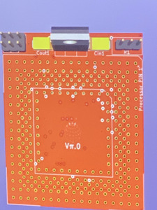
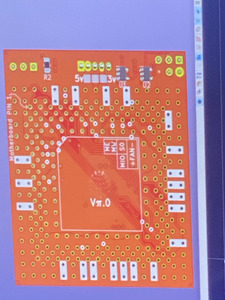
I wish to include all relevant infos on the silk screen. But will wait for Feipoa to finish tests. Here is a preview of the pi.0
As you can see in gerber view silk isn’t covering pad in final CAD files
I added silk around the locations because of the fill proximity issue. These are in an area where fill is at a premium.
I was going to square off the pads to make the caps look nice but that led to less fill cross section and other issues so I went back to round pads
Feiopa,
Is there enough room for four caps near the regulator? It’ll be tough but I may be able to move them toward socket and add two more pads
Btw, these caps for the pins, non polarized right?
I can see the problem. Not enough vias for power plane and ground. I'm talking about isolated vias not other than for pins as vias (not enough current handling), and relying on power plane for rest.
The examples of vias next to pads for capacitors:
http://www.sigcon.com/Pubs/news/6_09.htm
The ideal design is several vias to connect to inner layers for power planes around the regulator's pins, capacitor pads with 1 or 2 vias each. May have to enlarge the PCB little more by 30%, to make room for vias. Regulator needs lots of vias to connect to rest of power planes, and two tantalums gets their vias too. Are you now on 4 layers, may consider go 6 layers.
The practice is inner layers get power and ground, next is buried tracks going other ways and around the power and ground vias and then top and bottom mixed of power planes and ground planes and tracks. But you need to bridge the power planes to make connections at one end to another.
Spikes that look tall and thin can be instantaneous in order of around 20A to 50A in nanoseconds even for this little CPU of yours during CPU loaded heavily. With higher power CPU and GPU the instantaneous current goes up so much like 200A or more in nanoseconds.
This is typical design of APU with this capacitors and many vias look like, I know this is extreme.
https://guide-images.cdn.ifixit.com/igi/S5Uno … 5g5uVSO6HM.huge
https://guide-images.cdn.ifixit.com/igi/QiyYG … B2mVAtCcxy.huge
Cheers,
Great Northern aka Canada.
draw a pic of your suggested modifications. we are already 6 layer
https://www.researchgate.net/figure/Compariso … ts_fig4_3364576
https://electronics.stackexchange.com/questio … r-traces-and-gr
https://www.intel.sg/content/www/xa/en/suppor … /000084801.html
This is power and ground via connections to connect to the planes from vias style do you have this in your PCB design software? This is cross style.
https://www.altium.com/documentation/altium-d … tyle?version=21
Cheers,
Great Northern aka Canada.