Reply 20 of 32, by tsalat
Deunan wrote on 2024-04-19, 18:36:That's expected in a system with no ISA cards, and in general these signals are rarely used. Both should be H and they are. RESE […]
tsalat wrote on 2024-04-19, 17:31:IO CH RDY and IO CH CK are looking the same
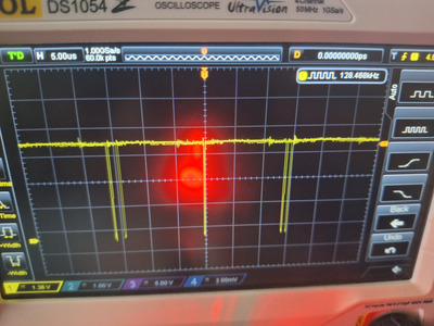
That's expected in a system with no ISA cards, and in general these signals are rarely used. Both should be H and they are. RESET is noisy but held L and well below 0,8V so in spec. Everything else seems in spec. MEMR appears dead but it can't be, the other lines toggling mean there is a program executing. I guess you run this with cache chips populated? In which case there might not be memory fetches if the cache always hits. CLK looks odd but it could be either triggering issue or some clock streching to hide memory refresh maybe. Hard to tell from one photo.
The F245 is used here to drive the upper address bits, the 16-bit ISA slot extension works a bit differently. But as I've said you don't need to worry about that now, we want to get the 8-bit part of the slot working first.
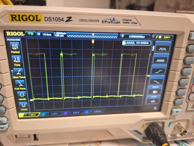
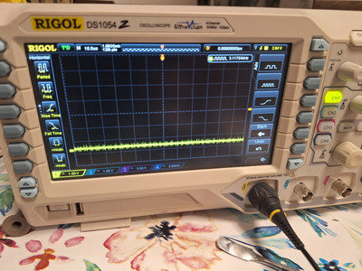
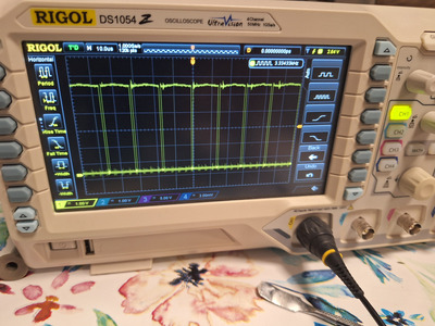
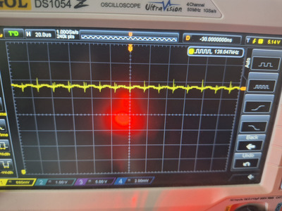
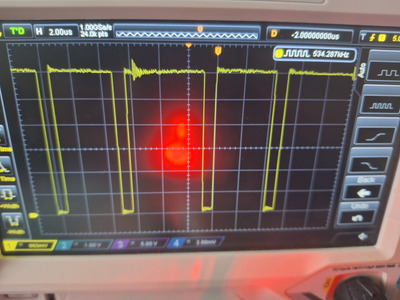
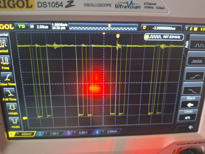
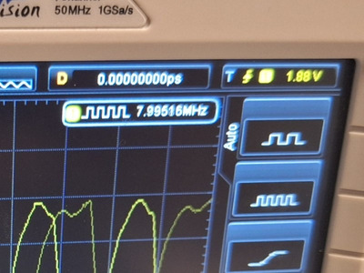
I did notice you changing the trigger level on some signals, please don't do that. You are only capturing the ringing noise and it's hard to tell from the photo if there are any actual logic transitions. In fact I now that I look at your earlier report about the address signals I see the same thing so now I'm not so sure that all the bits flip or not. There is one photo that shows only noise and no state changes. So please re-test the ADR00 to ADR19 lines again, no need to photo everything. If you see something like on photos 1,2 and 4 then it's OK. But photo 3 is an example of inactivity that should not really happen during normal operation. The code might just be in such a loop that a particular address line will not change but's that's unusual so write all those down if you see it.
thank you for your answer, sorry for the OSC changes, I have used the auto function and thus it resulted in it.
I have checked the Adr00 - Adr19 signals once more, screens below. The Adrxx is from a pin between the Adr19-10 (not sure which one), but most of the pins toggling between the noise and signal. Some more, some less, i.e. the noise is present most of the time with a signal appearing for a moment.
- yes, the cache is populated, not all slots but half of them
tomas