VOGONS


P55c at Overclocked to 300mhz?

Topic actions

Reply 198 of 237, by Mystery

User metadata
Rank Member
Rank
Member

Alright, I'm digging this thread out again, because I did a little experiment with a bunch of CPUs I got.

I collected six 233MMX CPUs to see how big the differences in the required VCore settings were when trying to achieve 300MHz.
Well, I had seven, but one was DOA 🙁

n4W0K.png
There are a few extra CPUs here. Two 200MHz P55C, one 233MHz which seems to be defective and the 266MHz Tillamook I tested earlier.
(click for larger version)

While I expected some variation in the results, I wasn't quite ready for the huge differences in CPU quality I got.

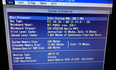
I used this system as a base for the whole experiment:
Board: DFI P5BV3+. An excellent Super7 board, but the FSB only goes up to 100MHz and the highest multiplier is 3.5
I used quality SDRAM at the most insane performance settings
The GPUs used are a Matrox Mystique and a Voodoo1
OS was DOS with Win98SE
The cooler I used is a full copper low profile So754 cooler with arctic ceramique thermal paste.

DOS Benchmarks used:
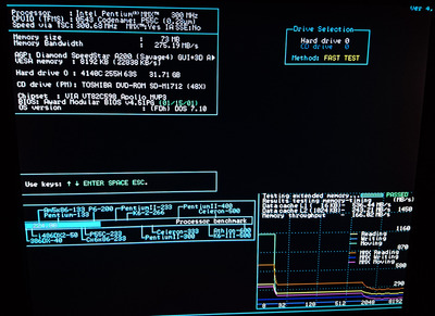
Speedsys
Quake1 (demo1)
PCPlayer Benchmark
3DBench
Shiny Benchmark (perf_dos)

In Windows I just ran a quick round of the "four" benchmark in Quake3 Arena.

If a CPU posted, I could usually run all benchmarks in DOS except for Quake1. Quake1 usually took an .1 or .2 VCore increment. I've found the IO-Volt setting to have a very small effect on the overall stability, so I usually left it at 3.3V.
Even if the Quake1 benchmark finished, Windows was another hurdle. It often took another .1 or .2 volts to get a stable desktop and sometimes an additional .1 volt to get the Q3A benchmark to run without errors.

I tested various settings and ran benchmarks for each of them.
250MHz @3x83
250MHz @2.5x100
266MHz @3.5x75
285MHz @3x95
290MHz @3.5x83
300MHz @3x100

I quickly realized that the 83MHz FSB had some problems as the benchmark results were terrible and even the 290MHz was slower than the 266 @3.5x75.
I also couldn't boot into Windows with the 75MHz FSB, no matter what the multiplier and vcore setting was. I suspect it's a problem with the PCI raid controller I had installed since the 75MHz FSB reduces the PCI Bus speed to 30MHz. Just a theory.

Because every CPU was able to run at 250 or 266MHz without any problems and the 83Mhz FSB didn't offer reasonable performance I just tested the 285 @3x95 and 300 @3x100 settings on all CPUs for the required voltage.

Btw: The speedsys CPU score doesn't really tell you anything about the system performance in games.

Alright, first the benchmarks:
PG81o.png
FSB is King! The P55C runs perfect @100MHz FSB and the boost from the higher FSB is much higher than a few extra MHz.
Look at the difference between 250MHz @2.5x100 and 266MHz @3.5x75.
Q3A isn't really a benchmark score you could compare, as the game runs at ultra low settings. It's just for testing the stability under Win98.

Now, let's get to the interesting part, the VCore settings.
I always started with the 3x95MHz setting at 2.8V, tried to see if it posted and if it didn't, I increased the VCore by 0.1V until it did. After the CPU posted I could usually run all benchmarks except for quake, which took another 0.1V. As mentioned before, getting Windows stable often took another 0.1 or 0.2V.
Most CPUs can easily reach 285MHz with the 95MHz FSB. If your P55C can't get to 300MHz and your board has both the 95 and 83MHz FSB available, go for the 285MHz @3x95 instead of 290MHz @3.5x83. It's 5MHz less, but it's still faster due to the higher FSB.
I often didn't have to fiddle around with the VCore too much, as I quickly reached a stable Windows.

Continuing with 300MHz, the picture changed. Getting the extra 15MHz often required a huge investment in extra VCore and even then some CPUs didn't reach a stable desktop. Since my board only offered 3.5V, I had to stop there.

Here's the chart:
K2Ogg.png
For the CPU Model I just took the last digits of the number above the copyright so I was able to distinguish them from one another.
As you can see, there are really REALLY big differences, even at 285MHz. Two CPUs were able to run 285MHz with the default VCore, which really impressed me. The last CPU didn't even get an error free Windows desktop, although it was stable.
The 300MHz data is the most fascinating one. Two CPUs immediately crashed, even at the highest VCore setting. I suspect the first CPU would run with 3,7V, but the last one is just hopeless. You'd have to fry it with more than 4V to get a stable Windows desktop.

Now, two CPUs stand out. They both ran 285MHz with the default 2.8V setting and required REALLY low settings for 300MHz. One ran with 3.3V, which is pretty low compared to other CPUs in this thread.
But the other (fifth in the chart) is just insane. I couldn't believe it and had to check the jumper settings three times, but that monster ran @300MHz with the default VCore of 2.8V! I'm not joking!

I'm pretty sure I could run this bad boy at 350MHz with this board, but I honestly don't want to ruin the CPU by putting too much power through it.

hET55.png
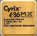
The holy grail of P55C CPUs? (click for larger version)

I have made one observation which might be useful, but it might just as well be a coincidence, because I didn't have a lot of CPUs to test.
Most P55C CPUs have "MALAY" printed on the back, but both of the "high performers" had "A4" printed there instead.

So there you have it.
For high performance, get the highest FSB possible, even if the speedsys CPU score suggests lower performance due to less overall MHz.
The quality of the 233MHz P55C CPUs varies greatly. I'd say theres as much as 1V difference (or more) to get CPUs running at 300MHz.
I got 3 out of 6 CPUs to 300MHz with a stable Windows desktop and Q3A benchmark.
One was close (almost stable), one would probably just need an extra .2V and one is utterly hopeless.
And 1 or 2 of the tested CPUs have the potential to go to 333MHz or even 350MHz at "reasonable" VCore settings.

Oh and if you try to get to 300MHz you should use quality components:
The mainboard is probably the most important piece. Make sure it's got a divider to keep the AGP/PCI bus at 33MHz (or slightly above/below that). Older boards don't offer this feature.
Check for a high FSB. It'll give you higher performance at lower clock speeds and it ensures L2 cache stability.
Get a board with SDRAM support and quality SDRAM. If you have 133MHz DIMMs that are detected by the mainboard, you can usually run them at the absolute fastest settings possible. The older PS/2 EDO SIMMs and even slower SDRAM DIMMS might cause trouble when running the system with a high FSB.

Now, I'd really like to confirm my theory about the MALAY/A4 233MHz P55Cs. Maybe I'll buy some more CPUs, but it's getting somewhat expensive. 😉

Now, if you have any questions or would like other tests or benchmarks to be performed, let me know.
I'll probably try the 3rd CPU in the chart @3.5x95 and 3.5x100, but I'm not going to harm the one in the photo above, it's just too precious 😉

IIRC feipoa wanted some Quake2 benchmarks. Which settings and demo should I use to have results you can compare to yours?

::42::

Reply 200 of 237, by nforce4max

User metadata
Rank l33t
Rank
l33t

Who knows it may have existed at one time. I do remember reading several times that a DDR chipset was designed for super 7 but it ever went into production. Did it have agp 4x maybe but I would have to go back and hunt it down again.

On a far away planet reading your posts in the year 10,191.

Reply 201 of 237, by kool kitty89

User metadata
Rank Member
Rank
Member
nforce4max wrote:

Who knows it may have existed at one time. I do remember reading several times that a DDR chipset was designed for super 7 but it ever went into production. Did it have agp 4x maybe but I would have to go back and hunt it down again.

DDR on SS7 would bit pretty pointless except maybe for multiprocessing . . . and the P55C was the last S7 CPU line to even support SMP.

OTOH extending SS7 chipsets to 133 MHz and maybe AGP4x would have made more sense alongside late-gen S370 boards, but as it is no SS7 chipsets or CPUs were ever rated for anything above 100 MHz, let alone 133. (though a handful of boards allowed overclocking to 133 with a 1/4 PCI divider)
It might have made sense for VIA to do that had they targeted S7 for the Cyrix III. (with the lower prices of S7 boards making more sense for such a low-end CPU, and the board-level L2 cache to compliment the 128k L1)

Reply 202 of 237, by nforce4max

User metadata
Rank l33t
Rank
l33t
kool kitty89 wrote:
DDR on SS7 would bit pretty pointless except maybe for multiprocessing . . . and the P55C was the last S7 CPU line to even suppo […]
Show full quote
nforce4max wrote:

Who knows it may have existed at one time. I do remember reading several times that a DDR chipset was designed for super 7 but it ever went into production. Did it have agp 4x maybe but I would have to go back and hunt it down again.

DDR on SS7 would bit pretty pointless except maybe for multiprocessing . . . and the P55C was the last S7 CPU line to even support SMP.

OTOH extending SS7 chipsets to 133 MHz and maybe AGP4x would have made more sense alongside late-gen S370 boards, but as it is no SS7 chipsets or CPUs were ever rated for anything above 100 MHz, let alone 133. (though a handful of boards allowed overclocking to 133 with a 1/4 PCI divider)
It might have made sense for VIA to do that had they targeted S7 for the Cyrix III. (with the lower prices of S7 boards making more sense for such a low-end CPU, and the board-level L2 cache to compliment the 128k L1)

Even SDR was a bit pointless considering just how slow the memory controllers were in all the chipsets produced for S5 and S7 when considering the bandwidth potential of the ram used. EDO has a bandwidth potential at 66mhz of 266mb/s but rarely achieved over 100-125mb/s. As for SDR it could have hosted two P55C with plenty to spare and could have gone quad if the memory controller was on par with 815E. In the end I am glad that AMD and Intel when for IMC over past designs.

On a far away planet reading your posts in the year 10,191.

Reply 203 of 237, by kool kitty89

User metadata
Rank Member
Rank
Member
nforce4max wrote:

Even SDR was a bit pointless considering just how slow the memory controllers were in all the chipsets produced for S5 and S7 when considering the bandwidth potential of the ram used. EDO has a bandwidth potential at 66mhz of 266mb/s but rarely achieved over 100-125mb/s. As for SDR it could have hosted two P55C with plenty to spare and could have gone quad if the memory controller was on par with 815E. In the end I am glad that AMD and Intel when for IMC over past designs.

Peak bandwidth also isn't going to get reached in real-world tests (even optimized benchmarks) unless the system caters to the specific operating parameters specific to the RAM in question. You'd need continuous burst/page-mode access to reach that (ie only accessing consecutive memory locations within the same page/row in the DRAM chips), and anything beyond that will incur significant performance penalties with latency from page-changes (change in row address). The greater the number of row changes, the greater the reduction in bandwidth. (granted, modern tricks like interleaved access to multi-bank DRAMs or multi-bank modules helps too)

So you've got limitations based on how software utilizes memory as well as the chipset and the CPUs themselves. (I think Cyrix's linear burst caching had more potential to approach peak DRAM bandwidth, though real-world examples would still be chipset and software dependent)
And you've still got timing parameters to consider on top of that. (moreso with EDO or -especially- FPM)

The performance gains in intel's Slot 1 and S370 chipsets obviously shed more light on how big a factor chipset performance is, comparing the various SDRAM based platforms of the time. (though, the same is true for comparing faster and slower systems using EDO DRAM)

On a related note, with the relatively weak SDR performance of SS7 boards, 50 ns EDO DRAM may have been a very good match for those 100 MHz chipsets. 100 MHz DRAM controllers would tend to mesh very well with the ideal timing (pulses) for typical 50 ns EDO chips. (maybe getting relatively close to the 400 MB/s peak potential of that RAM)
That would be something interesting to try out on an MVP3 board with SIMM sockets (like a VA503+) and compare that to performance of SDR on the same platform (as well as either types of RAM on slower buses), assuming the MVP3 chipset allows running EDO with a 100 MHz clock.

Interestingly, wikipedia specifically gives a 50 ns EDO DRAM timing example using a 100 MHz bus/controller.

Reply 204 of 237, by feipoa

User metadata
Rank l33t++
Rank
l33t++

I spent about 2 weeks reading this whole tread when the time permitted. It did not seem as if there was a clear answer on setting a 4x multiplier on P233 MMX chips. It was noted that the BF0 and BF1 pins should be shorted to set 4x. Another comment was to short BF0 and NC for 4x. RG100 tried both of these but did not check the actual CPU speed, for example, with Chkcpu or in Windows. He relied soley on the BIOS table look-up information at boot, which may not display the correct CPU speed if that speed is not in the table.

On the vintage-computer.com thread, there was much talk of running this 4x experiment, but nobody posted any photo evidence of 4x working on a non-Tillamook chip. Tetrium mentioned he was going to try this, but did not follow through in the vintage-computer thread.

I don't have any P233 MMX chips or S7 motherboards to kill for this test so I will not be trying this myself. Has anyone successfully run a P233 MMX at 4x and have photo evidence of it, for example, a CPU photo, chkcpu, and a benchmark? The best bet for this test is to try something modest, like 66x4 (266 MHz) at the rated voltage. It seems a lot of people who tried this 4x test were gunning for 300 MHz and above. Even 66x4 would might be of moderate benefit since you don't need to overclock the PCI bus for running the chip at 75x3.5.

Plan your life wisely, you'll be dead before you know it.

Reply 205 of 237, by retro games 100

User metadata
Rank l33t
Rank
l33t

Good post, feipoa. One of my many regrets, and funnily enough one that popped in to my head only the other day, was to check the actual CPU speed, rather than to solely rely upon the BIOS POST look-up info table. At that time, my naivety on this subject got the better of me, and I didn't appreciate that that look-up table could state an inaccurate CPU speed.

Reply 206 of 237, by Tetrium

User metadata
Rank l33t++
Rank
l33t++

I know this is old, but I think this thread is very informative. I somehow ended up reading the entire thing and the A4-bit prompted me to have a look at my own MMX chips to see what the deal could be with these markings and their supposedly better overclock.

I don't have a testbench available at this time, but I did write down the markings of all the MMX chips I had stored in a couple trays and noticed a few things that might be of interest.

What I wanted to know, is if there was anything peculiar about the "MALAY" marking or the "A4", and apparently all the ones with the MALAY marking were made in a fab in Malay (big surprise there). The line below the MALAY line starts with an "L", which is the fab's code, and the ones with "A4" start with a "C" (indicating these chips were manufactured in the USA).

I found a webpage with information about the Pentiums here, it lists the fabs where any particular chip is produced.

Now I know the sample rate of only 3 A4 chips isn't much, but at first I thought perhaps these chips were better overclockers because of a later production date?
But it seems the A4 MMX's might simple be of better manufacture, which might make these better overclockers. Otoh, my oldest A4 chip (I only checked all my 200's and 233's and skipped the CPGA and 166MHz models) had a production date of 721 (1997, week 21, Pentium MMX 200) and the newest 838 (1998 week 38, Pentium MMX 233), while the oldest MALAY chip I had was from 726 (1997 week 26) and the most recent one was apparently produced in 037 (2000 week 37!). My 3 most recent chips also had a different font compared to all the other chips from either factory, dunno what the story is with that.

These 3 chips (date codes of the other 2 are 907 and 913) were all 3 made in the MALAY plant and have the same font used on all my Tillamooks (which apparently also were made in the Malay plant).

The superchip from Mystery has a date code of 818 (C818, the C is the plant code btw. Malay uses L), which may have been a more recent production date.

In theory, newer chips should be better overclockers.

Here's the list of all the MMX chips I checked (200MHz and 233MHz only)
Apparently all MALAY chips were made in the L plant and all A4 chips were made in C plant (perhaps I missed a single chip, but all of the chips I had my eyes on, followed this simple rule)
233 L907 (Tillamook font)
233 L037 (Tillamook font)
233 L913 (Tillamook font)
233 L808
233 L746
233 L726
233 L823
233 L726
233 L805
233 L805
233 L814
233 L805
233 C829
233 C815
233 C801
233 C838
233 C829
233 C836
233 C749
233 C733
233 C829
200 L804
200 L739
200 C731
200 C807
200 C722
200 C745
200 C721

Whats missing in your collections?
My retro rigs (old topic)
Interesting Vogons threads (links to Vogonswiki)
Report spammers here!

Reply 208 of 237, by Tetrium

User metadata
Rank l33t++
Rank
l33t++
Jade Falcon wrote:

It doesn't tell us anything specific about that particular chip though.

Is this you btw?

Whats missing in your collections?
My retro rigs (old topic)
Interesting Vogons threads (links to Vogonswiki)
Report spammers here!

Reply 210 of 237, by Tetrium

User metadata
Rank l33t++
Rank
l33t++
Rhuwyn wrote:

Interesting thread. Makes me want to checkout my PentiumMMXs I have sitting around. Don't have nearly as many as Tetrium but I believe I have a couple.

Well, considering shipping costs was so significant and the chips themselves were so cheap, I figured I might as well get myself a life-long supply of these kinda great chips 😁

I never got around to actually doing any of those tests, just like I have so many other projects left unfinished years later.

I do have the idea that the Tillamook might have problems when the motherboard can cache over 64MB and I have a hunch (which may very well be incorrect!) that if it's possible to change the motherboard cache from WB to WT (which should be a bit slower, but doubles the amount of memory the motherboard can cache (works mostly on older Socket 7 motherboards though)), these Tillamooks may be able to cache up to 128MB, which should be enough to build a nice 400MHz Tillamook rig around.

(Yes, I am doing a lot of guessing here).

Whats missing in your collections?
My retro rigs (old topic)
Interesting Vogons threads (links to Vogonswiki)
Report spammers here!

Reply 211 of 237, by NostalgicAslinger

User metadata
Rank Member
Rank
Member

Maybe interesting for somone:

I have found a mobile Pentium MMX CPU with 200 MHz, 2.45V, manufactured in week 25/1998 (https://www.cpu-world.com/sspec/SL/SL2Z8.html). It runs fine on any desktop mainboard and also has a free mutliplier until 3.5x. This CPU runs fine with 300 MHz (100 FSB x3) and is completely stable with 2.8V (Prime 6+ hours run tested, 2.7V was only bench stable). CPU Cooler was a SPIRE FalconRock II CPU cooler with CoolerMaster thermal compound!

Reply 212 of 237, by Dmetsys

User metadata
Rank Member
Rank
Member

..

Last edited by Dmetsys on 2020-12-04, 17:09. Edited 1 time in total.


A7N8X-LA | 2800+ | GeForce2 MX400 | Audigy 2 ZS
BE6-II 1.0 | PIII-933 | Viper 770 TNT2 | Live 5.1 Value
MS-5169 | K6-2 450 | Voodoo3 3000 AGP | AWE64 Value
P5A-B | P200-S | 64MB | MGA Millennium | Yamaha 719
LS-486E | Am5x86-P75

Reply 213 of 237, by NostalgicAslinger

User metadata
Rank Member
Rank
Member
Dmetsys wrote on 2020-12-04, 16:44:

Yep, the Tillamook mobiles were impressive overclockers. You can also find fake "Pentium MMX 300 MHz" CPU's from China, which are overclocked Tillamook 233 MHz CPU's.

The mobile 200 MMX SL2Z8 stepping has a normal P55C (mxB1 stepping) core and also works fine with all desktop mainboards and enabled L2 cache. This is not a Tillamook CPU.

L_00002252.jpg

Reply 214 of 237, by Katmai500

User metadata
Rank Member
Rank
Member

Holy bump from 4 years ago Batman!

That is an interesting CPU though. There’s a whole Tillamook thread about getting L2 cache working on desktop boards, but this is a nice alternative for a fast Pentium MMX build.

Reply 215 of 237, by Dmetsys

User metadata
Rank Member
Rank
Member
Katmai500 wrote on 2020-12-05, 20:12:

Holy bump from 4 years ago Batman!

That is an interesting CPU though. There’s a whole Tillamook thread about getting L2 cache working on desktop boards, but this is a nice alternative for a fast Pentium MMX build.

If I ever find one of these CPU's, I'd be tempted to throw it into my P5A-B to see how far it can be pushed.


A7N8X-LA | 2800+ | GeForce2 MX400 | Audigy 2 ZS
BE6-II 1.0 | PIII-933 | Viper 770 TNT2 | Live 5.1 Value
MS-5169 | K6-2 450 | Voodoo3 3000 AGP | AWE64 Value
P5A-B | P200-S | 64MB | MGA Millennium | Yamaha 719
LS-486E | Am5x86-P75

Reply 217 of 237, by NostalgicAslinger

User metadata
Rank Member
Rank
Member

Here are some screenshots (only with cellphone camera):

Pentium MMX 01.JPG
Filename
Pentium MMX 01.JPG
File size
1.08 MiB
Views
1508 views
File license
Fair use/fair dealing exception
Pentium MMX 02.JPG
Filename
Pentium MMX 02.JPG
File size
1.07 MiB
Views
1508 views
File license
Fair use/fair dealing exception
Pentium MMX 03.JPG
Filename
Pentium MMX 03.JPG
File size
568.4 KiB
Views
1508 views
File license
Fair use/fair dealing exception
Pentium MMX 04.JPG
Filename
Pentium MMX 04.JPG
File size
1.12 MiB
Views
1508 views
File comment
Mersenne Prime 23.9 after +5 hours with 300 MHz and 2.8V
File license
Fair use/fair dealing exception