So the ST 6x86 is another thing Red Hill's museum got wrong.
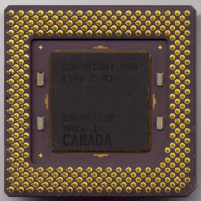
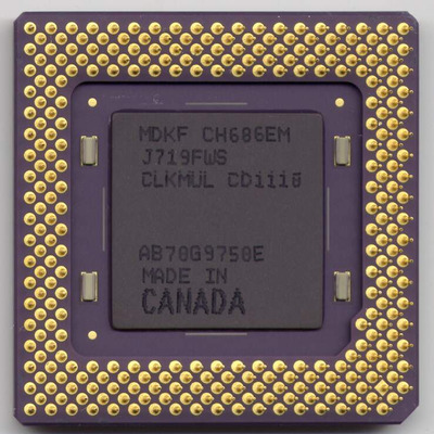
On the 5x86 manufacturing end: if IBM was manufacturing all the Cx5x86 cores, what's the deal with (apparently) only the 5x86C revisions being IBM branded and for that matter: no Cyrix branded 5x86C models. (or are late-model Cyrix 5x86s the same silicon, mask revision, etc, just marked and graded differently?)
It doesn't seem like IBM was just grading and marking their parts more conservatively given the actual chip functionality changed. Or am I mistaken and are IBM's 5x86 75 MHz parts equivalent to (at least some) 100 MHz Cyrix branded ones?
And for that matter, IBM started selling Cyrix based CPUs with their own IBM label on them starting with the 486DX2 (the Blue Lightning DX2 CPUs). So were those all IBM manufactured and were any of the ST branded 486s actually IBM produced?
I assume the 5V rated DX2 66 and 80 chips by ST were their own, but what about the DX4? Wikipedia lists that as being manufactured by SGST for a long time, but was it just sold through ST and just continued IBM manufacturing sort of like IBM's long-term 5x86 production?
Incidentally, I tried the 5V rated DX2-80 in that same Opti board and it wouldn't get past POST at 2x50 where I had a BL DX266 running at 2x50, apparently stable, but also open-bench 90 mm fan cooled (over both a heatsink and lots of airflow over the cache chips). The board is finicky at 50 MHz anyway, and I've had trouble with an Intel DX50 in it (but the bent pins might not make good enough contact in a non-ZIF socket and I'll probably save that thing for others) Besides that, with low wait states at 40 MHz, most performance is better there anyway. (memory bandwidth is mediocre even at 'zero' wait state DRAM configurations, but they do work at 40 MHz and gave generally better benchmarks at 2x80 than 2x50 with that BL)
It seems happy with that ST DX4 at 3x40, and an Avance Logic VESA card, too. It might do better at 33 MHz FSB and faster VLB settings, but I haven't messed with the video card's jumpers or the boards VLB selection at all. It's doing 3DBench at 55.5 FPS now. (and I was mistaken earlier, with the CL5422: it does 41.6 FPS in 3DBench 1.0 at 10 MHz ISA bus and 43.4 at 13.3 MHz. (the IDE drive seems fine at that clock rate now, too)
A CL5420 at 10 MHz in low wait state jumper mode does 43.4 at 10 MHz and crashes or gives lots of screen glitches at 13.3 MHz. (at 13.3 MHz with wait states on it does 43.4 as well)
PC Player was up to 12.5 FPS with the AL VESA card.
Quake at 320x200 was stuck at 7.7 FPS pretty much across the board, 7.6 worst-case with my ATi Graphics Ultra in 8-bit mode, 7.8 FPS best case with the low WS 10 MHz 5420 (I think I skipped that test on the VLB card). Doom varied a lot more, but the 8-bit mode performance loss was less dramatic than 3DBench or PC Player where were pretty much cut in half. (which makes sense since Doom does VGA RAM/register writes with 8-bit pixels or 2-pixel spans in low detail mode, and the other seem to be running in mode 13h and bottlenecks by the block-copy rate: though that doesn't say much for the VLB performance of this board ... and PCPlayer isn't 16-bit real-mode like 3DBench, so should be doing 32-bit copy operations, or maybe it also says the board has fairly fast ISA bus optimization and maybe DMA is being used, so ISA copies get buffered through chipset FIFOs and VLB might be limited to PIO and/or DMA is unbuffered and halts the CPU for entire transfers where ISA DMA allows more parallelism ... or I've just got unnecessary wait states enabled on the VLB card and/or board)
Anyway, this board is more of a 'fastest 386' sort of category (or would be if I could work out how to set the clock synthesizer to 50 MHz), or fast 486DLC. (I'll have to try to put a DLC40 and 487DLC40 or Fasmath together for some Pentium era benchmarks for that) My DLC40 seems to go fine, though I wouldn't expect it to actually do 50 MHz like some AMD DX40s can given the reputation for Cyrix chips running close to their limits.
That's probably what the OPTi 486SX (or DLX or similar variations) is best at. Fast 386-socket boards with full 486DLC support and 486SX/DX upgrade options. Maybe a bit like some of the Asrock boards oriented around flexible forward compatibility and legacy support: not great price to performance for a clean/new system build, but good for maching up mixed used (or cheap late-model old gen) parts and having flexibility for expansion. Moreso since a lot of slower rated, later production PGA Intel 386s as well as AMD's tended to overclock well, especially with a heatsink added. (like cases of DX20s used at 40 MHz, I've seen some anecdotes of PC shops setting up systems like that rather than end-user tweaks)
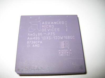
For AMD, I honestly thought a better move might have been to hedge their bets with a Socket 5 AM486 derived core, likely with a lot more L1 cache, sort of like an earlier WinChip. I think most engineering would be a new I/O block for the 64-bit wide P5 bus. Potentially even earlier than the 1995 launch of the .35 micron process x5 5x86. (a beefed-up .5 micron 486 derivative should've still used a lot less silicon than the .5 micron K5s)
That and pushing for voltage specs up to 4.0V. (ie getting good chipset and board vendor support for that) The AM486 core should've been low enough power to justify that where higher voltage on the K5 and 6x86 would have made them too exotic for the time. (PSU and board-level power concerns, plus the thermal issues)
I know NexGen resorted to 4.0V Vcore, but the Nx586 was both a smaller, less power hungry chip, and exclusively used on a proprietary board architecture.
As for the Cyrix FPU, I'd gotten a similar impression of the coprocessor core itself changing little or not at all (aside from refinements/tweaks specific to process changes) since the 386 or 486DLC days, but the I/O interface with the CPU core is where the changes were. (reducing latency and bandwidth bottlenecks; and with Cyrix's FPU already being fast that alone would've made a bigger impact than Intel or AMD's offerings: I think the AM486 had the more sluggish of the FPUs there too, depending on what operations and tests you compare, and I'm not sure the AM5x86 revision changed that much or at all, though I know Intel's DX4 had significant performance differences from the DX2, at least on the ALU end)
I'm not sure where the FIFO came in and if that was present from the first Cyrix 486DXs or not, but I could imagine that being one of the enhanced features added to the 5x86 core among the other tweaks/enhanced functionality, some of which were disabled and buggy, except on the 5x86C where they can usually be enabled without problems.
I do wonder how well the FPU scales or overclocks compared to the CPU cores of various 6x86 (M1 and M2) cores, especially given the FPU block took up less chip space and should have generated a minority of heat/power draw compared to the 486 and 5x86 (or Media GX). That and the MMX execution unit, which shares FPU registers anyway, and was kept relatively skimpy as well die-space and transistor budget wise, I think.
From my own experience, many of the Cyrix chips actually overclock quite well, sometimes at stock voltage (especially the 2.9V 250 nm IBM and NS chips), but get excessively hot compared to most or all other CPUs of their era when pushed to their max useable speeds. (though cooling sufficient for 3.2V K6 233s shoudl work well with contemporary 6x86 chips)
So assuming the FPU itself overclocks at least as well as the chip as a whole, they could've used different clock multipliers for the FPU and CPU and kept the core clock lower and relatively cool.
In 1995 and most of 1996 FPU performance would've been pretty marginal to target for mass market competition, and aside from regaining their former high-end FPU glory in the workstation market, Cyrix had little reason to bother with that (it was plenty fast for spreadsheet and office app calulation use and had the Pentium Fdiv bug PR mess to lean on as well)
But just slightly later, that PR-rating system would've scaled a lot better that way from 1996 onward (ie once games and multimedia applications became genuinely FPU-hungry and/or Pentium-specific FPU optimized) and more competitive with the Pentium II and Celeron. And honestly, beefing up raw FPU performance (one way or another) would've been more useful for the average end-user in 1996-1999 than having MMX or 3DNow! support at all.
That goes for the final revisions of the M1 6x86L as well. I'd think it would've made a good budget gaming capable CPU for 1997 with an overclocked FPU and voltage bump. They could've started speed-grading individual chips with overclockable FPUs and more conservatively rated CPU cores and potentially even gotten better yields by splitting them into Gaming+Multimedia and Business class variants.
(use pads on the package for surface-mounted jumpers to hard-code the multiplier set-up at the factory, or just use jumper-selection via the existing 2 select bits or add a third and re-use the existing PLL/clock generator logic on-chip: if you stuck with just 2 bits you could have 2x and 3x CPU core settings and a synchronous and 'fast' FPU settings.
so fast FPU would be : 2x CPU + 3x FPU or 3x CPU + 4x FPU)
It also took an oddly long time to get 100 MHz FSB parts out. I'm not sure if that (and the 2.9V rating) were aimed at compatibility with older and lower-end boards of the time or if there's stability issues more than I've experienced with my P5AB.
(I've got a couple MVP3 boards I can try now that might shed light on this, and I did a bit on a Shuttle Shuttle HOT-591P which didn't want to even post below 2.9V on my PR366 at any speed I tried, but seemed to work at 300 MHz at 2.9V for the bit I tried; that board had some corrosion on it though and some other oddities, like the voltage selector jumpers replaced by a single jumper block that toggled between 2.0 and 3.5V only, and no voltage warnings in POST or BIOS readings ... worse given it came with a K6-2 installed and 3.5V seems to kill those pretty much instantly, probably depending on the exact board and VRM configuration)
The P5A I have also tends to undervolt 250 nm Cyrix chips well (and K6-2s and P55Cs) will POST at stock 250 MHz down to 2.0V, but isn't stable enough to boot windows (or maybe if at ~40C, like a cold boot, but then would obviously crash quickly as it warms up ... or needs a beefy, out of era cooler), but in any case it does work at 2.2V in that same board, but probably needs to stay cooler than the rated temps.
(it eventually freezes or crashes in my AT case when there was no exhaust fan other than the 2001-era ATX PSU's, and a wimpy and very choked intake fan, when the case was closed up, but never did that with the case open, though I've had similar issues running K6-2s or 2/3+s at stock speeds under those conditions ; I had mostly flawless results a few years back when I was doing all my tweaking tests in a makeshift test-bench or coverless case and some tests with a propped up 90 mm fan blowing on a fanless heatsink)
And the M2 core might not have scaled well, but it at least had decent real-world performance at the scaling and yields it did manage ... compared to the Centaur C3 that VIA chose over it. (or chose over the enhanced, sort of K6-III-like Jalapeno or Joshua core, but that also took up more die space where the 180 nm plain old MII-400/433 was slightly smaller than the 180 nm C3 and seems to be about 2x the speed per-clock in the overall 6x86 testing ... but even further ahead in FPU-bound stuff) So I'd have thought the genuinely cheap option would just be keeping the SS7 based M2 core in production, and do simple die shrinks for late-gen embedded use. The Winchip 2 also did better per clock, but not as well as the M2 and also didn't scale as high in clock speeds.
(I suppose the C3 still had advantages in super low power, notebooks and thin clients like the Media GX/Geode was used for ...the C3 maybe did the performance per watt thing better in VIA S370 based systems than an M2 would in an MVP4 based integrated board, but I'm not sure how chipset power consumption compares, even if the MVP board omitted the board-level cache)
But this is way far afield of the 486 and 5x86 era topic now. (though I suppose that poorly ventilated AT case observation is worth noting for 486 era stuff, too: fanless baby AT and XT clone cases ... also carpeted floor mounted, not desktop mounted, but that's how Dad set-up all of our PCs back then too: under-desk tower/mini-tower, or a horizontal case tucked way under desk drawer areas, or inside TV cabinets, though he did other cooling mods and fan additions: and started cutting away all the fan cages/guards on PSUs and case exhaust ports by the time it came to Athlon XP era rigs)
Actually that old ATX PSU in the AT case has it's fan guard cut away, but airflow still wasn't good enough. (or probably pulls to much through other cracks and across the drive bay rather than over the board)