Reply 60 of 64, by CoffeeOne
mkarcher wrote on 2023-01-03, 11:19:There are three things you need to get a properly working L1 WB system. […]
CoffeeOne wrote on 2023-01-03, 10:36:Can you confirm (found it in a message from pshipkov)
.... pin B13, connected to +5V -> L1 WB enabled.Is that all is needed for Am5x86 setting L1 to WB?
There are three things you need to get a properly working L1 WB system.
....
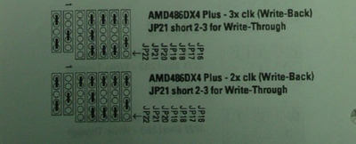
On the VL/I-486SV2GX4, this is accomplished by setting JP16 3-4 (for SRESET), JP17 2-3 (for INV) and JP18 2-3 (for HITM).
......On the VL/I-486SV2GX4, this can be enabled by setting JP16 1-2.
.......
Hi, thx again, but now I am a bit confused. Are we talking about the same mainboard?
What you wrote does not fit to the board at all?
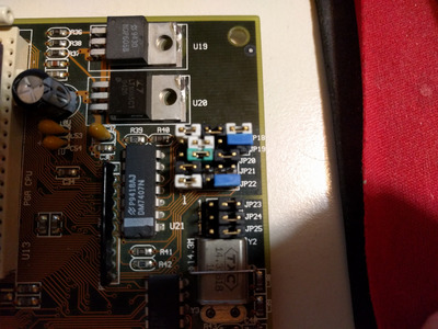
I have JP16: 1-2 and 4-5,
JP17: 1-2, 5-6
JP18: 1-2,5-6
I think for L1 WB JP21 is important on VLI Rev.2.x
EDIT: @mkarcher.
So there are 3 different jumper settings, 1.7 and 1.8 are different, too?
So sorry, you were talking about 1.7 I guess.
It is confusing.
Remark:
I played around with the jumper settings: I found a lot of possibilities to get no signs of life with an AM5x86. WTF. The board still works though, I will try to restore the settings that Am5x86 worked with L1 WT and 4 multiplier.