VOGONS


Reply 1100 of 1195, by MikeSG

User metadata
Rank Member
Rank
Member

The manual for the AP7363 Volt Regulator recommends to place 10uF's on both sides as close as possible to 5v-in and 3v-out to "ensure stability". So I'm going that route, and placing a few 0.1uFs on specific pins.

I'll post results in a few weeks.. I want to order & test it before posting photos/renders.

Reply 1101 of 1195, by Sphere478

User metadata
Rank l33t++
Rank
l33t++

Tony359 may be featuring the interposer in a video soon, heads up.

Sphere's PCB projects.
-
Sphere’s socket 5/7 cpu collection.
-
SUCCESSFUL K6-2+ to K6-3+ Full Cache Enable Mod
-
Tyan S1564S to S1564D single to dual processor conversion (also s1563 and s1562)

Reply 1102 of 1195, by MikeSG

User metadata
Rank Member
Rank
Member

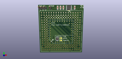
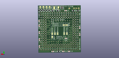
This is my version of the interposer.

It's designed to be compatible with the TI486SXL, TI486SXL2, as well as Intel & AMD 486SX, 486SX2 with jumper changes.

The design is untested as the sockets won't arrive until April, however it IS finished and possible to build using other sockets.

I don't have anything left to update on it (updated 12 Mar 2024), so I'm posting it now. Anyone can build and test it, minus the sockets, or wait until ~April to see me build & test it.

Images attached: 3D renders and the 168pin press-fit socket.

Gerber files are also attached for PCB manufacture.

PCB design requirements:
Length: 51.562
Width: 46.736
Layers: 4
Material: FR-4. 1.6mm
Min track/spacing: 6mil / 0.15mm
Min hole size: 0.3mm
Edge connector: no
Finished copper: 1oz
Inner copper: 1oz
Vias: No blind/buried vias present

Bill Of Materials (BOM):
Resistors:
-R1, R3, R5, R10 - 20k - RT0805DRD0720KL
-R2, R11 - 100r 0.5W Thick Film - CRCW0805100RFKEAHP
-R4 - 4.42k Thin Film (<=0.5% tolerance) - RT0805BRD074K42L
-R6, R7, R8, R9 - 2.2k Thin Film (<=0.5% tolerance) - RT0805BRD072K2L
Capacitors:
-C1 10uF - CL31B106KAHNFNE
-C2, C3, C4 - 3.3uF - CL31B335KAHVPNE
-C5 to C16 inclusive - 0.1uF - C0805C104K5RACTU
VR: AP7363-SP-13 (SO-8EP)
IC1: SN74LVC1G58DBVR (SOT-23-6)
IC2 (CLK): 74LVC2G74 (SOT-505-2)
XU1: 132pin 550-10-132-14-071101
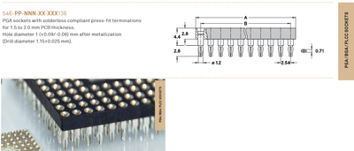
XU2: 168pin press-fit 546-83-168-17-101136

Sockets are only available from mouser at a high price. I didn't want to hand-solder rows, so the 132pin is a complete socket interconnect, and the 168pin is a press-fit (image attached). The availability currently is 23 for the 168pin, and 29 for the 132pin sockets, available on 19 April 2024. If they run out you need to wait another four months.
XU1: 132pin (550-10-132-14-071101): https://au.mouser.com/ProductDetail/Preci-dip … vOFry3q6Q%3D%3D
XU2: 168pin press-fit (546-83-168-17-101136): https://au.mouser.com/ProductDetail/Preci-dip … xAJb6r7AQ%3D%3D

Other info:
-Voltage is selected by the solder jumpers on the back. 3.3v, 3.6v, 3.9v, 4.2v. If none are jumpered, voltage is 4.5v. If more than one is jumpered, the lowest voltage is used.
-Solder pads on reverse side that operate FLUSH#: HLDA/M-IO and MEMW/SO, and are only required if you use them. The smaller pad under HLDA/M-IO is HLDA (CPU), used for testing 486sx CPUs that don't have MEMW and don't respond to Cyrix software.
-MEMW# single large through-hole is connected directly to the CPUs MEMW#.
-NA-SEL# default is jumpered 1-2 or NC.
-IC2 (CLK) is only required if testing a 486SX CPU.
-Underneath the VR/Volt Reg, a 5v pad is close-by the output in case the VR isn't used, so it can be solder-jumpered to output 5v. If 5V is used C1-10uF isn't required.
-If the VR/Volt Reg is used, the ground pad underneath needs to be soldered.

To configure for Intel & AMD 486SX. (NMI is the only difference between Intel & AMD):
1) 5V: Bypass Volt Reg if required.
2) CLK/CLK2# select. 486SX or TI486SXL.
3) BUSY#: 486SX: NC. TI486SXL: 1-2.
4) SUSP#: 486SX: NC. TI486SXL: 1-2.
5) SUSPA#: 486SX: NC. TI486SXL: 1-2.
6) SMADS#: 486SX: NC. TI486SXL: 1-2.
7) PEREQ#: 486SX: NC. TI486SXL: 1-2.
8 ) ERROR#: 486SX: NC. TI486SX): 1-2.
9) NMI#: AM486SX: 1-2. i486SX/TI486SXL: 2-3.
10) MEMW# (large through-hole on interposer): NC.
11) Use FLUSH# IC & pads on reverse side of interposer. The smaller pad under HLDA/M-IO is HLDA (CPU).
-a) If HOLD# is always sent to the CPU during DMA/master cycles, solder the larger pad HLDA/M-IO to the smaller pad HLDA (CPU), and solder MEMW# from the ISA bus.
-b) If HOLD# is NOT always sent to the CPU during DMA/master cycles, solder HLDA# and MEMW# from the ISA bus/Cache-Memory Controller. Leave the smaller pad unconnected.

Intel/AMD 486DX & 586 may work using AM486SX settings. FERR# and IGNNE# are not connected.

9/10 Jan 2024: Updated solder jumper pads for CPU. Support for AM486SX.
15 Jan 2024: Updated resistor values for voltage selection. 3.3v, 3.6v, 3.9v, 4.2v. No jumper = 4.5v.
12 Mar 2024: Cosmetic update. Updated note about smaller solder pad on reverse side (see note in 'other info' above).
May 2024: PGA-168 footprint update. VCC cap vias. (pending)

Attachments

Last edited by MikeSG on 2024-05-01, 10:51. Edited 26 times in total.

Reply 1105 of 1195, by MikeSG

User metadata
Rank Member
Rank
Member

The 74LVC2G74 chip (used as a clock divider to convert CLK2 to CLK) may allow 486DX, 586, POD cpus to work as well, but they should have a separate interposer design. I'm up to 10 pins that needs jumpering to suit them... They have a legacy FERR/ERROR output pin, and an IGNNE pin. So there's possibilities for those.

Reply 1106 of 1195, by Sphere478

User metadata
Rank l33t++
Rank
l33t++

Very interesting! Love it! Especially the ambition for other chips!

Interesting choice for regulator. 1.5a? Looks like. Little small🤔 at 3.6v that’s a max wattage of 5.4w I don’t recall the TDP of chips in question, but isn’t it right around 5w? 5v chips of course are direct wire, no reg.

I double dare you to get a POD running on this! :p
Fingers crossed!

Sphere's PCB projects.
-
Sphere’s socket 5/7 cpu collection.
-
SUCCESSFUL K6-2+ to K6-3+ Full Cache Enable Mod
-
Tyan S1564S to S1564D single to dual processor conversion (also s1563 and s1562)

Reply 1108 of 1195, by MikeSG

User metadata
Rank Member
Rank
Member
Sphere478 wrote on 2023-12-31, 17:11:

Interesting choice for regulator. 1.5a? Looks like. Little small🤔 at 3.6v that’s a max wattage of 5.4w I don’t recall the TDP of chips in question, but isn’t it right around 5w? 5v chips of course are direct wire, no reg.

I double dare you to get a POD running on this! :p
Fingers crossed!

The volt reg is very small (~5mm x 4mm x 1.5mm) but the central thermal pad is supposed to be soldered to the PCB which is then used as a heatsink. There's a smaller version (2mm x 3mm x 0.6mm) in a DFN2030-8 package that somehow meets the specs as well... may get warm but they're within spec...

If a 486DX interposer is made the Volt Reg should support up to 2 amps... The DX4-100 uses 1.45 amps. The AM5x86-133 uses 0.9 amps.

Would be interesting to get a POD running.. I don't have one though 🙁

Reply 1109 of 1195, by MikeSG

User metadata
Rank Member
Rank
Member
pshipkov wrote on 2023-12-31, 17:33:

But it sounded like you consider DX variant.
How will this work with onboard 387 fpus ?

Still looking through it...

For both 486sx and 486dx onwards the 387 FPU should be removed...

For 486dx & onwards CPUs, there's a legacy FERR# pin that takes the place of the 386 & FPU's ERROR# pin, and a IGNNE# pin (Ignore numeric error) that takes the place of the BUSY# pin.

Some information about it here: https://flylib.com/books/en/3.356.1.157/1/

FERR# may need to connect to IRQ13 (required for the CPU to decode the error), and/or connect FERR# to IGNNE# through a resistor (100r-2k) so that errors activate the ignore. Both are active low but IGNNE has a minimum set up time.

Other option is to not connect FERR# and IGNNE# and to disable FP errors in the FPU registers via a program.

Reply 1110 of 1195, by MikeSG

User metadata
Rank Member
Rank
Member

Updated the interposer design above (9 Jan 2024), after double checking AM486SX pins.

NMI# was on the pin next door, so as well as adding TI486SXL/i486SX and AM486SX selection, I changed all 386 specific pins to solder jumpers so they can be completely disconnected.

Intel & AMD 486DX compatible CPUs may work using the AM486SX settings. FERR# and IGNNE# are not connected.

Reply 1111 of 1195, by Sphere478

User metadata
Rank l33t++
Rank
l33t++

Love it! Keep up the tweaking! Can’t wait to see the results of tests!

Sphere's PCB projects.
-
Sphere’s socket 5/7 cpu collection.
-
SUCCESSFUL K6-2+ to K6-3+ Full Cache Enable Mod
-
Tyan S1564S to S1564D single to dual processor conversion (also s1563 and s1562)

Reply 1112 of 1195, by Sphere478

User metadata
Rank l33t++
Rank
l33t++

https://youtu.be/yVg2pvyYbn0?feature=shared

Interposer featured in a vid.

Sphere's PCB projects.
-
Sphere’s socket 5/7 cpu collection.
-
SUCCESSFUL K6-2+ to K6-3+ Full Cache Enable Mod
-
Tyan S1564S to S1564D single to dual processor conversion (also s1563 and s1562)

Reply 1113 of 1195, by Sphere478

User metadata
Rank l33t++
Rank
l33t++

So what’s the full scoop on scsi and clock doubling.

Has a dma scsi card been discovered that doesn’t have this glitch?

Sphere's PCB projects.
-
Sphere’s socket 5/7 cpu collection.
-
SUCCESSFUL K6-2+ to K6-3+ Full Cache Enable Mod
-
Tyan S1564S to S1564D single to dual processor conversion (also s1563 and s1562)

Reply 1115 of 1195, by feipoa

User metadata
Rank l33t++
Rank
l33t++

I recommend doing all baseline testing with a 5V PGA-132 TI486SXL2-50. This will rule out any soldering/contact issues. I haven't had any detrimental SCSI DMA issues at 2x with L1 and L2 enabled for which cyrix.exe could not resolve.

Plan your life wisely, you'll be dead before you know it.

Reply 1116 of 1195, by Sphere478

User metadata
Rank l33t++
Rank
l33t++

Saw this, haven’t dug too deep, anyone know what the extra circuit is?

Attachments

  • IMG_2845.jpeg
    Filename
    IMG_2845.jpeg
    File size
    144.98 KiB
    Views
    307 views
    File license
    Public domain

Sphere's PCB projects.
-
Sphere’s socket 5/7 cpu collection.
-
SUCCESSFUL K6-2+ to K6-3+ Full Cache Enable Mod
-
Tyan S1564S to S1564D single to dual processor conversion (also s1563 and s1562)

Reply 1117 of 1195, by Paralel

User metadata
Rank Member
Rank
Member
Sphere478 wrote on 2024-03-20, 14:49:

Saw this, haven’t dug too deep, anyone know what the extra circuit is?

Now that is quite interesting. I've never seem a mod like that. It's an excellent implementation of a minimal mod.

Reply 1118 of 1195, by RayeR

User metadata
Rank Oldbie
Rank
Oldbie

Hm, some 6MHz ceramic resonator and counter that probably divides it to some lower frequency, no idea...
If it would be a PLL for main clk then it would make a sense...

Gigabyte GA-P67-DS3-B3, Core i7-2600K @4,5GHz, 8GB DDR3, 128GB SSD, GTX970(GF7900GT), SB Audigy + YMF724F + DreamBlaster combo + LPC2ISA

Reply 1119 of 1195, by rasz_pl

User metadata
Rank l33t
Rank
l33t
Sphere478 wrote on 2024-03-20, 14:49:

Saw this, haven’t dug too deep, anyone know what the extra circuit is?

I think I saw same cpu + weird interposer on os2museum long time ago

Open Source AT&T Globalyst/NCR/FIC 486-GAC-2 proprietary Cache Module reproduction