Reply 160 of 1184, by SpikeyPsyche
Rank
Newbie
So... What ever happened with this project? I've been watching it from the sidelines, but then nothing. I was really excited to see the outcome.
So... What ever happened with this project? I've been watching it from the sidelines, but then nothing. I was really excited to see the outcome.
Project is pending someone with sufficient PCB design experience, interest, motivation, and time to produce the gerber files. I've tried to begin learning KiCAD but am disrupted every 13 seconds with noise, screaming, fighting, COVID-home schooling, or many various other requirements of servitude. Even when the kids are sleeping, at least one of them wakes up screaming about some nonsense, so I am left doing computer activities which requires little thought and compliment constant disruption.
Plan your life wisely, you'll be dead before you know it.
feipoa wrote on 2020-04-20, 17:53:Project is pending someone with sufficient PCB design experience, interest, motivation, and time to produce the gerber files. .
What's the status regarding schematics, netlist etc.? If you have a clear overview of that, I would probably be able to do the layout, in Orcad PCB designer ..
Please use the "quote" option if asking questions to what I write - it will really up the chances of me noticing 😀
The previous poser, cb88, who began work on this had uploaded some files in this post: Re: Custom interposer module for TI486SXL2-66 PGA168 to PGA132 - HELP!
I'd suggest skimming through the whole post though, as much information is buried in the commentary. You're probably looking at a 4-layer minimum PCB with a design freq. from 66-100 MHz. If that's too much of a constraint, then 66-80 MHz @ CLK2.
There's been some discussion (started by Tiido) about using two PCB's and interconnecting them, but seems to me that this will increase trace lengths and not make for an as compact design, but may be easier for the home assembler with limited tools. My thoughts are more in line with cb88 on the design though, that is, one PCB. Could always do two designs. I think if 80, 90 MHz or even 100 MHz is going to work, best keep traces to a bare minimum.
EDIT: one problem with putting the project off too long is that those cheap ($15 ish) and readily available SXL2-66 chips may sell out, or the seller fold up shop.
EDIT2: I think distributing at least 100 of these units into the Vogons and CPU-World communities would be fairly easy, that is, assuming they work.
Plan your life wisely, you'll be dead before you know it.
So, long story short .. I looked at the post you refer - opened the pdf, as I'm not too fund of installing KiCAD on my work computer 😉 It seems that the task is to interconnect a PGA-132 male socket to a PGA-168 female and a voltage regulator. No glue logic necessary? Do we have any idea if it will actually work? Is the SXL2-66 bus compatible out of the box or?
If it's that easy, I'll be happy to look into the work of routing and creating gerber files ..
Please use the "quote" option if asking questions to what I write - it will really up the chances of me noticing 😀
Yes, mostly. I'd read the thread though. If I recall right, it worked on my wire wrap mess at 4 MHz (1st page of thread), but I couldn't boot because the diskette timing was messed up or something of that nature.
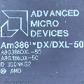
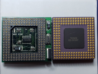
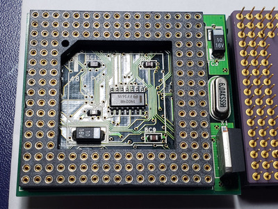
You can also take a look at this sandwich in which I use the SXL2-66 in a VRM interposer on a PGA-386 interposer. I was able to get it working up to 66 MHz on most motherboards. Re: Custom interposer module for TI486SXL2-66 PGA168 to PGA132 - HELP! I think the PGA-168 to PGA-132 in that photo is from Improve-It. While it contains some glue logic, I traced it out and it only seems to affect the FLUSH# pin. This seems to be some sort of cache invalidation circuit. Contains some NAND gates and a ripple counter which from what I can tell, is counting clocks until it is reset with the Master Reset input. I believe these were added to increase compatibility with some obscure 386's and is not necessary. A software invalidation approach is built-in to the CPU (BARB) and from my tests, was just a few realtics slower in DOOM compared to the hardware flush method. Most newer 386 boards have the hardware flush method built onto the motherboards. The SXL2 series should already have the NAND flush circuit built in, but may require a connection to MEMW#. BARB can be instead though. In the thread notes, I mention to include a pin header for MEMW#.
All of this is discussed in detail in the thread notes. I'm going from memory here, so best to look at the design notes. The only difference between the PGA-132 version of the SXL2 and the PGA-168 version of the SXL2 is the FLT# pin, MEMW# pin, and the PGA-168 includes the built-in flush circuit. The PGA-132 version has worked fine on all 386 motherboards I've tested, which is about 8 boards, and that is without the built-in flush circuit. Refer to page C-4 and and D-3 of the SXL product book. The 66 Mhz version of the PGA-168 SXL2 runs at 3.6 V nominally, rather than 5 V like the 50 Mhz version. I mention to include a trimmer on the VRM to adjust the voltage for overclocking potential. I suppose you could also include discrete resistors and a dip switch under the PCB or inside the socket for voltage increments, e.g. 3.6, 3.65, 3.7, 3.75, 3.8, 3.9, 4 V, but it complicates the design.
Some design considerations are here in bulk, Re: Custom interposer module for TI486SXL2-66 PGA168 to PGA132 - HELP! , but they are all over this thread and I'd suggest looking through them as there is some challenge with fitting the PGA sockets, what to do with FLT# and VCC5, 5V fan header, etc.
Plan your life wisely, you'll be dead before you know it.
OK, I'll see if I can find a quiet time to trawl through the thread 🤣 From today until Tuesday, "only" 2 of our 4 kids are here 😉
Re: Custom interposer module for TI486SXL2-66 PGA168 to PGA132 - HELP! Seems pretty simple - all though it seems there is some oscillator and a couple of logic circuits? Is it actually more or less a copy of that - with a VRM we would want?
Please use the "quote" option if asking questions to what I write - it will really up the chances of me noticing 😀
Yes, but we don't need any of the logic circuits that are on the Improve-It module (That's the module with offset PGA-132 socket)
We need a 3-pin header for MEMW#, 5V, and GND - the later 2 for a fan. The MEMW# pin as an option to connect it to MEMW# on the ISA bus if people want to experiment with the hardware flush method.
We should try to centre the PGA-132 and PGA-168, just like this other brand has done: Re: Custom interposer module for TI486SXL2-66 PGA168 to PGA132 - HELP!
We need a VRM with its required caps. I've noted a model I spec'ed in the thread. VRM needs a trimmer to adjust or a micro DIP swtich, or perhaps micro jumpers like found on SCSI HDDs. As the VRM takes up about the same space as the trimmer, just as well use a trimmer on the side of the PCB that is a little wider. So in place of that oscillator, a trimmer. Should be enough space for the larger VRM's cap and a 3-pin header on that ledge as well.
We need decoupling caps where appropriate.
The rest of the pins should be one-for-one from PGA-132 to PGA-168, except FLT, MEMW#, and VCC5.
Should all the address and data traces need to be the same length?
Kids - I guess it depends on your kids. I found the transition from dealing with 3 kids substantially more involved than 2 kids. Girls are also much easier to deal with pre-puberty compared to boys.
Plan your life wisely, you'll be dead before you know it.
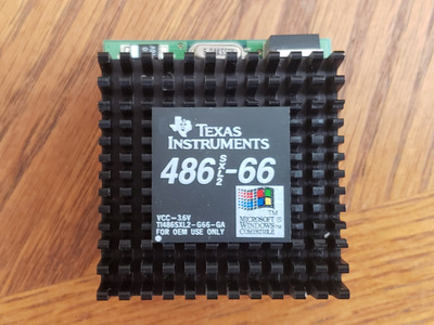
feipoa wrote on 2019-08-22, 22:06:A CPU collector sent me some photos of another SXL2-66 upgrade, this time PGA-168 with VRM. This is what we're trying to replic […]
A CPU collector sent me some photos of another SXL2-66 upgrade, this time PGA-168 with VRM. This is what we're trying to replicate, minus the unnecessary extra circuitry. This adapter uses an EZ1086CM as the VRM. I have never seen one of these adapters in person or in photograph until now, so I suspect it is exceedingly rare.
386_SXL2_Upgrade_1.jpg
386_SXL2_Upgrade_2.jpg
386_SXL2_Upgrade_3.jpg
386_SXL2_Upgrade_4.jpg
386_SXL2_Upgrade_5.jpg
Hey, I also have one of these! If this is exactly what we're trying to replicate, I'm willing to lend/ sell it if it may help someone produce 100 more 😛 Otherwise it'd probably just sit on my shelf. I'm afraid of using something so rare for a long term gaming build.
Builds:
NScaleTransitModels wrote on 2020-11-19, 01:26:Hey, I also have one of these! If this is exactly what we're trying to replicate, I'm willing to lend/ sell it if it may help so […]
feipoa wrote on 2019-08-22, 22:06:A CPU collector sent me some photos of another SXL2-66 upgrade, this time PGA-168 with VRM. This is what we're trying to replic […]
A CPU collector sent me some photos of another SXL2-66 upgrade, this time PGA-168 with VRM. This is what we're trying to replicate, minus the unnecessary extra circuitry. This adapter uses an EZ1086CM as the VRM. I have never seen one of these adapters in person or in photograph until now, so I suspect it is exceedingly rare.
386_SXL2_Upgrade_1.jpg
386_SXL2_Upgrade_2.jpg
386_SXL2_Upgrade_3.jpg
386_SXL2_Upgrade_4.jpg
386_SXL2_Upgrade_5.jpgHey, I also have one of these! If this is exactly what we're trying to replicate, I'm willing to lend/ sell it if it may help someone produce 100 more 😛 Otherwise it'd probably just sit on my shelf. I'm afraid of using something so rare for a long term gaming build.
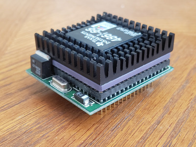
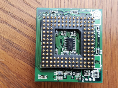
20201118_123640.jpg
20201118_123648.jpg
20201118_123708.jpg
If that allows it to run on a standard board with (or even without) Cyrix support, I would buy a couple. I don't know any 486 boards that run the SXL2, and would love to test mine. Have a few PGA132 I would like to test as well.
See my graphics card database at www.gpuzoo.com
Constantly being worked on. Feel free to message me with any corrections or details of cards you would like me to research and add.
Yup, that's it. Where did you find your upgrade? Are you willing to upload a photo of the top of the unit without the CPU installed? The bottom shows a NAND gate. There's also crystal, perhaps for the chip under the CPU? I don't think any of these are absolutely necessary.
It is unlikely that I'll get around to these CAD drawings. As time goes on, the time sucker of 3 kids gets worse and worse. Hopefully some will come along with sufficient PCB experience to whip these out with minimal head scratching.
It seems a few few folks have been liquidating their collections this year. If you are interested in selling, let me know. I'd like to see if this adapter can be taken up to 80, 90, or 100 Mhz reliably. It would serve as a good reference point to emulate. If it can work at 90 or 100 MHz, obviously there will be more interest.
Plan your life wisely, you'll be dead before you know it.
If the reproductions are like my example, they'll run on non-Cyrix boards. To answer both of you, I got mine attached to an early DTK 25mhz motherboard which was made well before the DLC chips. The seller (on Ebay) either wanted to get rid of it quickly or had no idea how rare these are 🤣. The SXL2 works on that board and a later 386 board I tried, though I haven't gotten around to extensive testing or benchmarks yet. However, it didn't fit onto my PCChips M326 b/c the CPU socket was too close to an ISA slot.
Photos coming up. Yeah not sure if the gates/ crystal are necessary, also note the empty "TC2" and "TC4" outlines on the bottom. I actually know a couple folks who I believe have PCB design experience, but they have their hands full and aren't crazy about retro tech. Either way, I'm definitely following this project and am interested in one, or two, or more interposers 🤣.
I'll PM you after I post my benchmarks; I'm doing another 386 build soon (parts in the mail) so that'll be a good time for some more testing before I let go of this thing. It would be interesting to see if this adapter works at 80 mhz or higher; we'd have potentially the fastest 386-class upgrade aside from the Transcomputer 486 module (unless there was a 100mhz Blue Lightning? I forgot) I would not be the one to overclock it though, I already fried a DLC-40 earlier this year at 50 mhz 😒
Builds:
Builds:
I am surprised you fried a DLC at 50 MHz. I had no issue with TI 486DLC's at 50 MHz.
An IBM BL3 at 100 MHz would be faster than the TI SXL2 at 100 MHz, but the BL3 is limited to 16 MB cacheable memory and it is extremely difficult to find an adapter that will work with a motherboard well. I have such a pair, but I could only get that BL3 up to 75 MHz on this particular board, and the adapter covered the VLB slots. So the SXL2 at 80-100 MHz would be more realistic in a broader range of boards.
So you're the guy who bought this upgrade adapter in the complete system I saw earlier this year on eBay? I had just missed that listing, but saw it a few days after it ended. The adapter was hidden well on the 3rd photo or something, and not zoomed in well if I recall. You got a good price for that complete system.
Plan your life wisely, you'll be dead before you know it.
I'm surprised as well since the chip wasn't at 50 mhz for long (it posted at 50, but wouldn't boot Win95). I confirmed it was bad after dialing it back to 40; it would crash upon reaching the Win95 desktop. But only with internal cache enabled, so I think the cache was fried.
It seems that someone on here managed to get a Blue Lightning working at 100 mhz? IBM Blue Lightning (486DLC)
He didn't specify which 386 board he used though. Also by "Blue Lightning 486DLC" he means the BL3, not the earlier SLC3 right? Sorry the naming is kind of confusing. If it was actually a SLC3, it would have been limited to 16mb addressable, an even bigger handicap than 16mb cacheable.
You might be thinking of another listing; I got mine on a standalone motherboard. It's still in my purchase history, the seller put "TI 486sxl2-66" in the listing title and the adapter was in plain sight. I jumped on it as soon as it listed because the price was on the low end, even for 386 motherboards in general.
Builds:
I could possibly see 40MHz parts burning out at 50MHz if they were from an earlier batch. I don't think the -40 was available on release....it came later.
The Blue Lightning has multiple names for whatever reason. BL3 and DLC3 are the same chip. Then you have the 168-pin blue lightning chips that are rebadged cyrix 486DXs.
The SLC3 and DLC3 were released at the same time as far as I know. They're the same chip with different bus interfaces.
I don't know how much of an impact the L1 cache in the blue lightning would have on overall system performance beyond 16MB....because L1 cache is used for both data and CPU instructions. So even beyond 16MB the L1 cache should still make a difference. I would think for memory intensive operations the L2 cache is more critical on a 386.
"Will the highways on the internets become more few?" -Gee Dubya
V'Ger XT|Upgraded AT|Ultimate 386|Super VL/EISA 486|SMP VL/EISA Pentium
I was able to get a different BL3 upgrade board working at 110 MHz on a different board, but this particular combination required flusing the L1 every I/O and this hurt performance.
Well that is reassuring, it means that perhaps there are more of these adapters out there than first thought. There was also one NIB which sold this year. That makes three in total.
Were you using a Cyrix or TI branded DLC?
There was definitely a performance hit when using more than 16 MB on the BL3. If I recall right, it dropped CPUMark32 results in half during my Win95 tests for HWiNFO and CPUID.
Plan your life wisely, you'll be dead before you know it.
I fried a TI-branded DLC, in particular a -40BGA, IIRC? I also have a /E-40GA that still works. Never quite understood what the difference was between those two designations, maybe the second one is a later iteration?
That is definitely good to know; I'll also keep an eye out for more adapters that may pop up.
I'd also think that the L1 cache shouldn't hurt performance so badly, especially if it's as big as 16kb. Have you tried running benchmarks with the L2 disabled?
Builds:
I think the /E might have some power saving features. It should be listed in the databook.
"Will the highways on the internets become more few?" -Gee Dubya
V'Ger XT|Upgraded AT|Ultimate 386|Super VL/EISA 486|SMP VL/EISA Pentium
Interesting thread about the upgrade with this cpu. Unfortunately on some boards there is not enough space around the 386 socket to place a PGA-168.
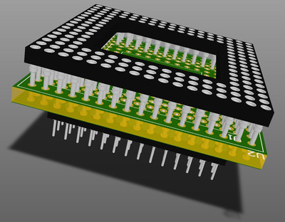
Out of interest I made a schematic with this pcb preview:
Since this is not a high-speed design with differential signals, all traces do not have to be of the same length. But it should still be short traces.
I would also provide two power planes for GND and 3.6V. The signal layer in between reduce EMI.
It's sure that the pins FLT # & MEMW # are not used? It would be good to check this against your interposer.
Niemand ist nutzlos, er kann immer noch als schlechtes Beispiel dienen...