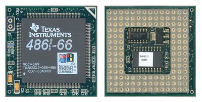
The PAL is probably essential for some older motherboards, which is why it is added on the module - to be more cross-platform compatible, particularly on boards which are not L1 cache aware. The TI 486SXL2 PGA132 is the same chip as your TI 486SXL2 QFP144, except that it runs at 5 V as opposed to 3.3-3.6 V. It makes sense that your PAL is interfacing with control pins, probably to hold the CPU while the cache is being updated/flushed on motherboards which are not L1 aware. When using the PAL on boards which are L1 aware is just redundancy. This is my theory. How do you explain why the PGA132 SXL2 works on my system and the PGA168 does not? They are the same chips, running at a different voltage. At least this is what the reference manual says. The caveat would be if TI changed something which is undocumented on the 66 MHz version of the chip.
You cannot get to know the PAL without the microcode. It is a programmable logic device. If you don't have a copy of the software which is written to the PAL, then how do you get to know the software?
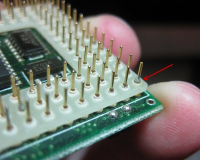
The less risky way to measure the actual voltage would be to solder a 30 AWG wire to the BB1117 and bring the wire out between the PGA pins to your voltmeter. Or if you are feeling on top of the world, you'd touch the QFP with a strand of thin wire while activated. If you aren't comfortable with any of these, I do not recommend doing it. Whether it runs at 3.3, 3.45, 3.6, or 3.65 V is not all that important. I can vary these on my module with a turn of the trimmer. I was just curious if the maker of the module may have found that 3.6 V too high, or too low and decided to run the unit at more/less voltage.
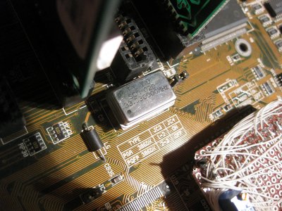
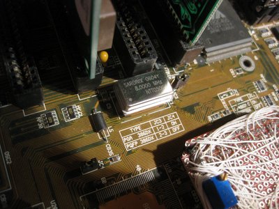
Vcc5 is different than Vcc. It is a special pin on the QFP and PGA168 modules, which is really strange. Under some conditions, the manual request 5 V coming to Vcc5, while all other Vcc pins are 3.6 V.
If I had your module in front of me, I would probably mount it in a third hand vertically, this way I could probe the QFP-144 side, and the PGA-132 side simultaneously.
Plan your life wisely, you'll be dead before you know it.