rasz_pl wrote on 2022-12-03, 19:15:inductor would only work if noise was coming from power supply (inductors block AC) […]
Show full quote
pshipkov wrote on 2022-12-03, 16:56:Hard to say anything concrete by just looking from the side, but usually adding a ferrite bead in serial to Vcc and something like 10-to-100mF capacitor to ground before or after it ?
inductor would only work if noise was coming from power supply (inductors block AC)
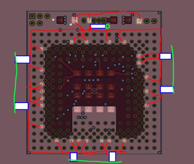
Sphere478 maybe something like this? yes it would make it wider on 3 sides to accommodate extra bypass caps :
lolpass.jpg
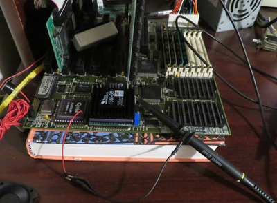
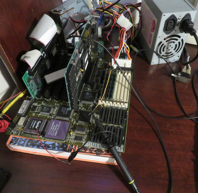
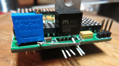
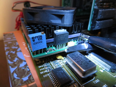
feipoa looking at photo from the side all the VCC3 pins are not obscured by bottom socket at all, bypass caps can be soldered directly to those pins externally on the bottom. 7-8 small ceramic caps.
but as it works I dont expect any design respins :)
It is slowly becoming more apparent that the issue somehow stems from the PCB or its cap placement. I think unless we can show some massive improvement with the existing alpha boards using whatever hackery, there would be little value in redesigning the PCB - unless someone else is paying for them. lol.
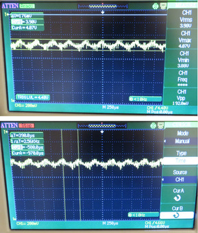
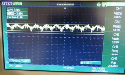
Rasz_pl, Yes, there are several points for which I could solder some caps to the bottom pints. I hope 0805 fits here. I'll see what sizes I have. What capacitance, 47 pF, 10 nF, 47 nF, 100 nF? And should I remove the centre region caps? I currently have a 10 uF cap for Cin because the LP VRM requests below 500 mOhm ESR.
Sphere478 wrote on 2022-12-03, 16:28:
Do I flip the center cap orientation?
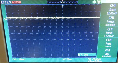
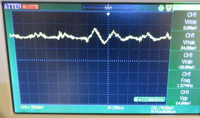
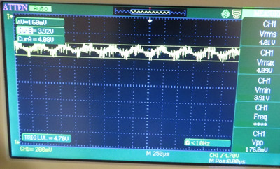
No. Checked before I got started. I also took scope photos without those caps installed.
Sphere478 wrote on 2022-12-03, 16:28:
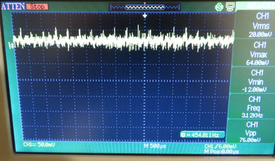
Idk, like the thing works. In fact it works just as well at least as a oem unit… I’m not sure what to make of this power plane noise thing…
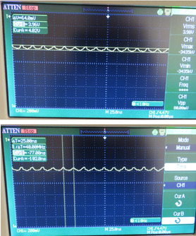
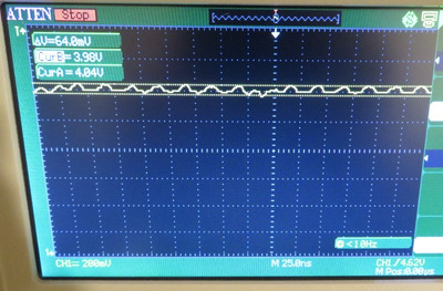
Not quite. Were you able to read the wall of photos? Using the same CPU, the OEM unit could overclock with 0.05 V less than the replica. I wouldn't call it a problem.
Sphere478 wrote on 2022-12-03, 16:28:
Btw, your bench psu test sounds like a farce. You had serious voltage drop it sounds like. Do it again with shorter, thicker wires please.
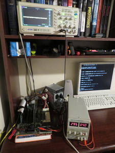
I see no value to gain from this. Using two different VRMs will have the shortest "leads" possible and the same oscillations occur. I am already using my shortest cable, which is probably falling apart at the clip unions due to age. However, if I were to hack together a 5" cable, what would it show? It would probably show less voltage drop, but the oscillations would still be there. Could a 2-ohm wire resistance cause oscillations like this, no, but they would create that deltaV.
Sphere478 wrote on 2022-12-03, 16:28:
Also, please scope your bench top psu under equal resistive load as a control.
Sphere478 wrote on 2022-12-03, 21:30:
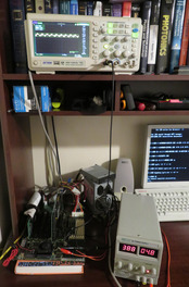
we need to be damned sure the bench psu control test was valid. So put the scope on that psu with a resistor and analize it to see if it is good enough to use, and do the test again with very thick very short wires
I'm pretty sure you are barking up the wrong tree here. I did this 5 years ago, and I my mind was much sharper back then. Refer to the resistive load measurements presented earlier for trials of different VRMs. If it is absolutely do or die for you, I'll run it again, but I feel it is a waste of effort.
The last thing I will do, after adding direct pin caps, is compare the MIC against the LP on this motherboard. If there's even a 50 mV improvement, we can use the LP instead, but they don't have a mounting hole option for the tab.
Plan your life wisely, you'll be dead before you know it.