VOGONS


Reply 880 of 1184, by pentiumspeed

User metadata
Rank l33t
Rank
l33t

Silkscreen misalignment is acceptable of this quality. I see this all the time.

Again, there is no copper D-pads to create solder pads for capacitors or resistors, under that silkscreen as you call them. Give a scrape into white silkscreen with a razor, you will know what I mean, I can tell. This is solderable vias without pad next to them.

I worked with PCB all the time at work and at home, and tv repair years ago. One of these was repairing cracked PCB by jumpering the breaks with pieces of wire.

Cheers,

Great Northern aka Canada.

Reply 881 of 1184, by Sphere478

User metadata
Rank l33t++
Rank
l33t++
pentiumspeed wrote on 2023-01-27, 17:38:
Silkscreen misalignment is acceptable of this quality. I see this all the time. […]
Show full quote

Silkscreen misalignment is acceptable of this quality. I see this all the time.

Again, there is no copper D-pads to create solder pads for capacitors or resistors, under that silkscreen as you call them. Give a scrape into white silkscreen with a razor, you will know what I mean, I can tell. This is solderable vias without pad next to them.

I worked with PCB all the time at work and at home, and tv repair years ago. One of these was repairing cracked PCB by jumpering the breaks with pieces of wire.

Cheers,

Idk where you are getting that we believe that there are pads under the silk. No one here believes that. (That I know of…) kicad does a pretty good job of cutting the silk out around the pad for the gerber generation.

These two examples shown recently in the thread mine and feiopa’s came in exactly as ordered spare some silk misalignment.
After some investigation on the last page
It was only my 3.3v board that came in wrong.

Sphere's PCB projects.
-
Sphere’s socket 5/7 cpu collection.
-
SUCCESSFUL K6-2+ to K6-3+ Full Cache Enable Mod
-
Tyan S1564S to S1564D single to dual processor conversion (also s1563 and s1562)

Reply 882 of 1184, by feipoa

User metadata
Rank l33t++
Rank
l33t++

pentiumspeed, you are correct, these are not proper SMD D-pads - they are through holes with a slight flare on the top and we are calling these "D-pad" for lack of a simpler term. What would you like to call them? Capacitors will be soldered between these through holes rather than creating proper SMD pads for convenience.

There is not supposed to be solder pads under the silk and there isn't. The silk is serving a few purposes
a) identifying the locations of Vcc & GND for SMD capacitors on the through-holes.
b) providing a few microns of height to move these SMD capacitors a bit further away from the surface.

I hope this clears up the confusion.

Plan your life wisely, you'll be dead before you know it.

Reply 883 of 1184, by pentiumspeed

User metadata
Rank l33t
Rank
l33t

Makes sense. Thank you.

It is slightly odd solder via, still. Hardly what I call these a pad as there is no neighboring solder pad attached to the via. Is there a capacitor or resistor large enough to touch these solder pins at their ends? If not, that means excess solder to make up for the gaps? Otherwise, this why needs to have some pads created next to via.

I have not seen anything like this, and the PCB designers where limited space, had pads right next to solder via or through holes and I see this often on RF tuner and small boards to solder SMD components onto these pads.

Have fun then.

Cheers,

Great Northern aka Canada.

Reply 884 of 1184, by Sphere478

User metadata
Rank l33t++
Rank
l33t++
pentiumspeed wrote on 2023-01-27, 23:20:
Makes sense. Thank you. […]
Show full quote

Makes sense. Thank you.

It is slightly odd solder via, still. Hardly what I call these a pad as there is no neighboring solder pad attached to the via. Is there a capacitor or resistor large enough to touch these solder pins at their ends? If not, that means excess solder to make up for the gaps? Otherwise, this why needs to have some pads created next to via.

I have not seen anything like this, and the PCB designers where limited space, had pads right next to solder via or through holes and I see this often on RF tuner and small boards to solder SMD components onto these pads.

Have fun then.

Cheers,

These locations were the best we could come up with. There really isn’t much space there. So we did what we could but we wanted capacitors there so we did this.

The capacitors fit quite nicely there if you scroll back some pages you can see we installed some previously on the last prototype

Sphere's PCB projects.
-
Sphere’s socket 5/7 cpu collection.
-
SUCCESSFUL K6-2+ to K6-3+ Full Cache Enable Mod
-
Tyan S1564S to S1564D single to dual processor conversion (also s1563 and s1562)

Reply 885 of 1184, by pentiumspeed

User metadata
Rank l33t
Rank
l33t
Sphere478 wrote on 2023-01-28, 00:00:
pentiumspeed wrote on 2023-01-27, 23:20:
Makes sense. Thank you. […]
Show full quote

Makes sense. Thank you.

It is slightly odd solder via, still. Hardly what I call these a pad as there is no neighboring solder pad attached to the via. Is there a capacitor or resistor large enough to touch these solder pins at their ends? If not, that means excess solder to make up for the gaps? Otherwise, this why needs to have some pads created next to via.

I have not seen anything like this, and the PCB designers where limited space, had pads right next to solder via or through holes and I see this often on RF tuner and small boards to solder SMD components onto these pads.

Have fun then.

Cheers,

These locations were the best we could come up with. There really isn’t much space there. So we did what we could but we wanted capacitors there so we did this.

The capacitors fit quite nicely there if you scroll back some pages you can see we installed some previously on the last prototype

I thought so, I have done same way with caps wedged between pins.

Cheers,

Great Northern aka Canada.

Reply 886 of 1184, by feipoa

User metadata
Rank l33t++
Rank
l33t++

ALPHA2 TESTING

I'll be beginning alpha 2 testing soon. I've attached photos of Alpha 1 next to Alpha 2. The smaller unit is Alpha 2. I guess we could call it Beta 1 if it works.

SXL2_PGA168_Alpha2_comparison_with_alpha1_A.JPG
Filename
SXL2_PGA168_Alpha2_comparison_with_alpha1_A.JPG
File size
647.21 KiB
Views
1061 views
File license
CC-BY-4.0
SXL2_PGA168_Alpha2_comparison_with_alpha1_B.JPG
Filename
SXL2_PGA168_Alpha2_comparison_with_alpha1_B.JPG
File size
706.63 KiB
Views
1061 views
File license
CC-BY-4.0

I haven't added the PGA pin caps or the centre caps yet. I was thinking to leave the central caps off for now and add 8x 100 nF PGA pin caps. Make this the starting point for testing and noise, then fill it up and re-measure in a few iterations. I will be using the low inductance probe, which requires quite a bit more effort and increases probability of short circuits as one hand holds the probe and the other the camera. The hand with the camera will also adjust the scope. Only had two shorts last time.

Yeah the scope can take its own images, but it cuts off the right column with data boxes, unless it is the first picture taken from a power cycle. Stupid buggy Chinese firmware.

Alpha 1, as shown, has:

Cout = 22 uF tantalum
Cin = 10 uF ceramic
central Cin = 10 uF, 100 nF, 220 nF, 10 uF: all ceramic
central Cout = 10 uF, 100 nF, 220 nF, 10 uF: all ceramic
PGA pin caps: 8x 100 nF, 3x 10 nF, 4x 47 pF: all ceramic

Alpha 2, as shown, has:

Cout = 22 uF tantalum
Cin = 10 uF ceramic
PGA pin caps: 8x 100 nF (yet to be added)

Last edited by feipoa on 2023-02-13, 10:54. Edited 1 time in total.

Plan your life wisely, you'll be dead before you know it.

Reply 888 of 1184, by Sphere478

User metadata
Rank l33t++
Rank
l33t++

Probably best to call it prototype one, two, and three 😀 you are showing prototype 2 and 3

Looks good! Can’t wait for results!

I have some parts coming for mine but may be a while before I get them.

Wow it really is a LOT smaller!

Need to put JLCJLCJLC under the pins somewhere to hide the jlc numbers from the final product.

Sphere's PCB projects.
-
Sphere’s socket 5/7 cpu collection.
-
SUCCESSFUL K6-2+ to K6-3+ Full Cache Enable Mod
-
Tyan S1564S to S1564D single to dual processor conversion (also s1563 and s1562)

Reply 889 of 1184, by feipoa

User metadata
Rank l33t++
Rank
l33t++

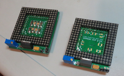
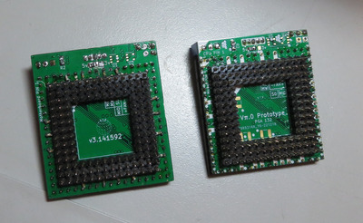
My read wire wound unit with the red protoboard would be the prototype/POC. The first JLCPCB unit would normally be called an "alpha" phase unit from my experience. It is semantics nonetheless.

I ran some tests with Alpha 2, but first I took a baseline with Alpha 1. The setup is slightly different from before - I have L2 cache installed now and am using a junky Trident board rather than an ET4000AX. The change in graphics cards was a precaution. The addition of L2 was for testing something else prior.

I took some baseline measurements with this slightly modified setup.

The trimmer was set such that Vout on the VRM reads 4.02 V on the DMM. This equates to 4.11 V max, 4.03 V min on scope with 10x probe. This translates to 4.08 Vrms on scope w/10x.

Recall from previous FFT measurements, the largest noise swing was at 5 KHz, the second largest at 80 MHz, so these are the two scales I will reference.

Alpha 1

Cin = 10 uF cer
Cout = 22 uF tant
central Cin = 10 uF, 100 nF, 220 nF, 10 uF
central Cout = 10 uF, 100 nF, 220 nF, 10 uF
PGA pins Cout = 8x 100 nF, 3x 10 nF, 4x 47 nF

NOISE TARGETS TO BEAT FROM ALPHA1
Vout
5 KHz : Vpp = 90 mV
80 MHz : Vpp = 42 mV

Vin
5 KHz : Vpp = 84 mV
80 MHz : Vpp = 18 mV

Alpha 2
Cin = 10 uF cer
Cout = 22 uF tant

Vout
5 KHz : Vpp = 426 mV OUTCH!

Alpha 2
Cin = 10 uF cer
Cout = 22 uF tant
PGA pins Cout = 8x 100 nF

Vout
5 KHz : Vpp = 128 mV

Vin
5 KHz : Vpp = 92 mV

It looks like there's at least 40 mV of noise we want to reduce. What do you guys think - first target the central regions with large 1210 sized ceramics, or target the rest of the PGA pins with 10 nF, 1 nF, 47 pF, etc caps? I was thinking to target the central core first, similar to how Alpha 1 was tuned.

Plan your life wisely, you'll be dead before you know it.

Reply 890 of 1184, by Sphere478

User metadata
Rank l33t++
Rank
l33t++

Yeah, baseline measurements without many caps are probably gonna be nuts on the noise.

Give the 5v in center a few caps and see what happens. One at a time. Get 5v as clean as you can, then move on to vout? Is my hunch.

Probably leave the three on the bottom empty till last.

Sphere's PCB projects.
-
Sphere’s socket 5/7 cpu collection.
-
SUCCESSFUL K6-2+ to K6-3+ Full Cache Enable Mod
-
Tyan S1564S to S1564D single to dual processor conversion (also s1563 and s1562)

Reply 891 of 1184, by feipoa

User metadata
Rank l33t++
Rank
l33t++

For some reason, all 1210 ceramic pads in the central regions (top and bottom) are for Cin. I don't recall this alteration. I thought it was to be half for Cin and half for Cout.

Plan your life wisely, you'll be dead before you know it.

Reply 892 of 1184, by Sphere478

User metadata
Rank l33t++
Rank
l33t++

That’s correct.

Center caps: all 5v (in)

Pga caps: all 3.3v (out)

At regulator: one 3.3v (out), one 5v (in)

Sphere's PCB projects.
-
Sphere’s socket 5/7 cpu collection.
-
SUCCESSFUL K6-2+ to K6-3+ Full Cache Enable Mod
-
Tyan S1564S to S1564D single to dual processor conversion (also s1563 and s1562)

Reply 893 of 1184, by feipoa

User metadata
Rank l33t++
Rank
l33t++

I don't recall there being a discussion on this change. This is a fairly large deviation between revisions. It is possible that we will not be able to reach the same noise levels as Alpha 1. The noise on Vout is mostly not originating from Vin.

Plan your life wisely, you'll be dead before you know it.

Reply 894 of 1184, by Sphere478

User metadata
Rank l33t++
Rank
l33t++
feipoa wrote on 2023-02-14, 04:55:

I don't recall there being a discussion on this change. This is a fairly large deviation between revisions. It is possible that we will not be able to reach the same noise levels as Alpha 1. The noise on Vout is mostly not originating from Vin.

Well, it certainly wasn’t a secret :p it was there to see in the screenshots all along.
give it a try! 😀

The reason for this:
Putting the 3.3v caps in the middle was a mistake. They need to be in the path of current as others mentioned, and we discovered. The pga pins, and near the regulator are the current path for 3.3v, this is where they should be, not the center. If you need more, stack on top of the regulator cap or the pga pins. This should give the best result for tests. After your tests, if it is determined you need more 3.3v cap pads, we can find a place for them. Larger pcb will likely be needed Or, Probably can place a (1) extra larger cap pad by the regulator underneath the pcb. But I suspect using all the pga pin capacitor locations will give you more than enough places to install caps. Hopefully the physical sizes and capacitance values match up with what is needed.

Many things changed from the last version. Hopefully for the better.

I do recall the noise was mostly on 3.3v from the processor its self. Solved with the pga pin caps mostly. If memory serves.

I suspect you’ll only end up needing half of the capacitor pads provided on the pga pins, and half in the center. But do your tests, see what we got.

Sphere's PCB projects.
-
Sphere’s socket 5/7 cpu collection.
-
SUCCESSFUL K6-2+ to K6-3+ Full Cache Enable Mod
-
Tyan S1564S to S1564D single to dual processor conversion (also s1563 and s1562)

Reply 895 of 1184, by MikeSG

User metadata
Rank Member
Rank
Member

What do you guys think - first target the central regions with large 1210 sized ceramics, or target the rest of the PGA pins

What does the Volt Reg manual say for capacitors on Vout? 2.2uF, 100nF?... If it's not stable it will transfer all through the CPU.

Also, every via/trace hole acts as a mini coil and reduces the effect of capacitors. 100nF capacitors should be right on the pin. 1uF+ can be a little further.

Last edited by MikeSG on 2023-02-15, 07:47. Edited 1 time in total.

Reply 896 of 1184, by rasz_pl

User metadata
Rank l33t
Rank
l33t
feipoa wrote on 2023-02-14, 03:40:

For some reason, all 1210 ceramic pads in the central regions (top and bottom) are for Cin. I don't recall this alteration. I thought it was to be half for Cin and half for Cout.

I specifically remember mentioning Cin caps are useless after spotting so many pads 😀

Open Source AT&T Globalyst/NCR/FIC 486-GAC-2 proprietary Cache Module reproduction

Reply 897 of 1184, by chjmartin2

User metadata
Rank Newbie
Rank
Newbie

Hi All. When this is done, it will allow which types of 486 chips to be used in a 386? Like, will you be able to use a 5x86 or a DX/4 in it? What clock frequency does it expect from the motherboard? I also have an Inboard/386 and have an interest because Transcomputer modules are impossible to find. Anyway, I have a Cyrix 25/50 but it is running 20/40. Big question for me, assuming all of this works, is would I be able to do better than that with this? I assume the 486 66 would end up being the same, running FSB at 20 Mhz and processor at 40 MHz. Regardless, this is a really cool community project.

Thanks,

Chris

Reply 898 of 1184, by debs3759

User metadata
Rank Oldbie
Rank
Oldbie
chjmartin2 wrote on 2023-02-18, 08:16:

Hi All. When this is done, it will allow which types of 486 chips to be used in a 386? Like, will you be able to use a 5x86 or a DX/4 in it? What clock frequency does it expect from the motherboard? I also have an Inboard/386 and have an interest because Transcomputer modules are impossible to find. Anyway, I have a Cyrix 25/50 but it is running 20/40. Big question for me, assuming all of this works, is would I be able to do better than that with this? I assume the 486 66 would end up being the same, running FSB at 20 Mhz and processor at 40 MHz. Regardless, this is a really cool community project.

Thanks,

Chris

It is only for the TI 486SXL2, which (in its PGA168 form) has a different pin configuration to other 486.

See my graphics card database at www.gpuzoo.com
Constantly being worked on. Feel free to message me with any corrections or details of cards you would like me to research and add.