VOGONS


First post, by RJDog

User metadata
Rank Member
Rank
Member

I almost feel stupid for asking this, but... do ya'll think it may be as easy as adding a 40 pin header to the unpopulated header position of a Yamaha YMF-719? I have (or soon will) a machine that only has a single IDE channel, so an expansion card with a secondary IDE port will be necessary to add a CD-ROM. Unfortunately the only card I have available that's close is a Yamaha YMF-719 but with IDE header unpopulated.

Look forward to your thoughts and criticism 🤣

Last edited by RJDog on 2017-10-16, 23:05. Edited 1 time in total.

Reply 1 of 23, by Deksor

User metadata
Rank l33t
Rank
l33t

I've got one which has an IDE port, I may take photos of it so you'll be able to compare it with yours and see if there is any component missing (such as a 0 ohm resistor for example that could be used as a jumper to enable the IDE capability)

Trying to identify old hardware ? Visit The retro web - Project's thread The Retro Web project - a stason.org/TH99 alternative

Reply 2 of 23, by RJDog

User metadata
Rank Member
Rank
Member
Deksor wrote:

I've got one which has an IDE port, I may take photos of it so you'll be able to compare it with yours

That would be super helpful! My plan was basically to test all the traces on the header to make sure they all went to an appropriate place to see if there was any other missing components; but that probably wouldnt help me with resistor values. Thanks!

Reply 3 of 23, by Jade Falcon

User metadata
Rank BANNED
Rank
BANNED

It's probably a lot more then just a header. Why would anyone remove a usable feature for $.50?
I would say there probably a ic that will need added to the card and maybe different firmware

Reply 4 of 23, by RJDog

User metadata
Rank Member
Rank
Member
Jade Falcon wrote:

I would say there probably a ic that will need added to the card

Maybe... but thats not the part that scares me.

Jade Falcon wrote:

and maybe different firmware

That's the part that scares me.

Reply 5 of 23, by Deksor

User metadata
Rank l33t
Rank
l33t
Jade Falcon wrote:

It's probably a lot more then just a header. Why would anyone remove a usable feature for $.50?
I would say there probably a ic that will need added to the card and maybe different firmware

I remember seing somebody soldering an AGP slot on a motherboard that lacked one and that worked flawlessly.

If removing this was only saving them up 0.5$, maybe they could overprice the model having an IDE connector ?

Trying to identify old hardware ? Visit The retro web - Project's thread The Retro Web project - a stason.org/TH99 alternative

Reply 6 of 23, by yawetaG

User metadata
Rank Oldbie
Rank
Oldbie

It could be anything, e.g.:
- OEM version of card
- cheap version of card that also lacked other features (drivers, other software) besides the IDE connector
- IDE connector turned out to have issues and was left off later revisions of card

As for the original question, adding the IDE connector might work, but without the card's firmware or the system's BIOS supporting a (secondary) IDE channel it might only work with drivers.

Reply 7 of 23, by RJDog

User metadata
Rank Member
Rank
Member
yawetaG wrote:

- cheap version of card that also lacked other features (drivers, other software) besides the IDE connector

Well, the CD that came with it literally only has the drivers on it, so... maybe that one?

Also, my mistake, the card is a YMF718-S, not YMF-719 as I remembered. I took a look at it, and every pin on the IDE connector terminates to a pin directly on the ISA card edge connector, or to a pin on the YMF718-S chip; there are apparently no missing components other than the connector. I'm going to try just soldering on a 40-pin connector...

Reply 9 of 23, by SaxxonPike

User metadata
Rank Member
Rank
Member
RJDog wrote:

I took a look at it, and every pin on the IDE connector terminates to a pin directly on the ISA card edge connector, or to a pin on the YMF718-S chip; there are apparently no missing components other than the connector.

This appears to be the case on both of my OPL3SA based cards as well. Give it a shot!

Sound device guides:
Sound Blaster
Aztech
OPL3-SA

Reply 10 of 23, by RJDog

User metadata
Rank Member
Rank
Member

I thought I would share the details of the quick study I did on the card; see attached photos. All but one of the traces to the 40-pin IDE connector go right to the ISA card edge connector, with the D0-D7 data lines shared with the YMF-718-S chip (and D8-D15 data lines solely for use with the IDE connector). This makes sense, as the IDE/ATA "protocol" is essentially ISA bus.

20170731_105154.jpg
Filename
20170731_105154.jpg
File size
1.76 MiB
Views
1856 views
File license
Fair use/fair dealing exception
20170731_105134.jpg
Filename
20170731_105134.jpg
File size
2.1 MiB
Views
1856 views
File license
Fair use/fair dealing exception

This site was particularly helpful in figuring out what was going on with the individual pins:
http://www.ele.uri.edu/courses/ele408/s2001/p … nd_ide/ide.html

So, based on that information, the tracing of the pins on the IDE connector, and the pins that don't go anywhere (no connection, no traces anywhere), it looks like the IDE connector should only support a single drive, with no DMA.

SaxxonPike wrote:

This appears to be the case on both of my OPL3SA based cards as well. Give it a shot!

Thanks! And, also, great link in your signature... not sure why I didn't see that before 😀

Reply 11 of 23, by Jepael

User metadata
Rank Oldbie
Rank
Oldbie
RJDog wrote:

All but one of the traces to the 40-pin IDE connector go right to the ISA card edge connector, with the D0-D7 data lines shared with the YMF-718-S chip (and D8-D15 data lines solely for use with the IDE connector). This makes sense, as the IDE/ATA "protocol" is essentially ISA bus.

It is basically ISA bus, but something has to do the address decoding for IDE /CS1 and /CS3 signals, if they go to YMF718 then it does the address decoding and needs to be told it should actually do the address decoding. Though sometimes /CS3 is not used.

Also the ISA signals are usually buffered with bus tranceivers such as two 74LS245 chips, just wiring ISA bus signals straight to IDE cable could do terrible things to signal integrity. Maybe that's why the card has no IDE connector because they determined it would not work?

RJDog wrote:

So, based on that information, the tracing of the pins on the IDE connector, and the pins that don't go anywhere (no connection, no traces anywhere), it looks like the IDE connector should only support a single drive, with no DMA.

IDE always supports two devices, nothing limits it to single drive only.
ISA bus IDE has never used DMA so that's normal.

Reply 12 of 23, by appiah4

User metadata
Rank l33t++
Rank
l33t++

For your reference this is my Addonics YMF-718 card with an IDE header:

gallery_60983_11505_445765.jpg

As far as I can tell the connectors go directly to the ISA slot.

Retronautics: A digital gallery of my retro computers, hardware and projects.

Reply 13 of 23, by RJDog

User metadata
Rank Member
Rank
Member
appiah4 wrote:

For your reference this is my Addonics YMF-718 card with an IDE header:

Sweet, thanks!

Jepael wrote:

but something has to do the address decoding for IDE /CS1 and /CS3 signals, if they go to YMF718 then it does the address decoding and needs to be told it should actually do the address decoding

There is an unpopulated 74SL138 that is connected to exactly those pins, so I assume thats what it is/was supposed to do. Directly adjacent is a 0-ohm resistor array to bypass it to the YMF-718-S, which is populated, so I assume the YMF-718-S is doing that function and the 74SL138 is not required.

Jepael wrote:

Also the ISA signals are usually buffered with bus tranceivers such as two 74LS245 chips, just wiring ISA bus signals straight to IDE cable could do terrible things to signal integrity. Maybe that's why the card has no IDE connector because they determined it would not work?

Yeah, I thought that as well, that it might have been an unstable feature so they removed it. Lots of examples of cards with the IDE connector in this configuration, so... we'll see.

Reply 14 of 23, by Jepael

User metadata
Rank Oldbie
Rank
Oldbie

Other cards do not have the LS138 decoder. It's possible it is needed for the wavetable part but I did not find any pictures with wavetable chips or LS138.

From your pictures it seems that if the resistor network RP1 has four 0-ohm jumper resistors, it connects some high order ISA address bits as IDE CS1 and CS3, which obviously can't work.

Other cards that do have the IDE interface at least has removed RP1 to disconnect IDE chip selects from ISA address bus, but also removed a 0-ohm configuration resistor RA2.
http://s192804805.onlinehome.us/images/1/5916 … WHA151A00-1.jpg

It's still unknown if you need other changes or reflashing the PNP ROM with new configuration that enables the Yamaha chip to actually decode the IDE interface chip selects to some specific address.

Reply 15 of 23, by RJDog

User metadata
Rank Member
Rank
Member
Jepael wrote:

Other cards that do have the IDE interface at least has removed RP1 to disconnect IDE chip selects from ISA address bus, but also removed a 0-ohm configuration resistor RA2.
http://s192804805.onlinehome.us/images/1/5916 … WHA151A00-1.jpg

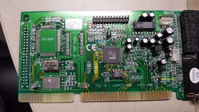
Great picture! It is exactly the card that I have... same FCC ID, etc., but with IDE interface. So, yeah, exactly as you point out, RP1 and RA2 are notably missing (both 0-ohm resistors), which are no problem to remove (I'll try it first with them in place and then removed). The one thing that has me concerned now is X3... the 24Mhz oscillator. It is present on your picture, but not on my card. It appears that the traces for it ultimately connect to pins 51 and 52 on the YMF-718-S. Not sure if this is related to or required for IDE functionality... notably, the picture of the card that appiah4 posted does not have the 24Mhz oscillator (and is the same YMF-718-S chip).

Reading more about the YMF-718-S chip itself (found a datasheet for YMF-715 which should be close enough I think http://www.alldatasheet.com/datasheet-pdf/pdf … HA/YMF715E.html) it seems that both the 33Mhz and 24Mhz clocks are used to generate a "master clock" in the chip... no mention of the 24Mhz oscillator being optional, but it doesn't seem to be related to the operation of the IDE interface at all. The 0-ohm RA2 seems to be connected to the XA24 pins, so perhaps that is present on my card because the oscillator is not present (where the opposite is true on your picture). The 0-ohm bridge RP1 is definitely related to the IDE though. The IDE device select and IRQ pins are connected to pins MP6, MP7, and MP8 on the YMF-718-S, which are, per name, multi-purpose pins based on selected configuration. One of the configurations (SEL=2) is to use the MP6,7,8 pins for higher address bits, so your comments line up about the IDE not working with the bridge present as it connects the chip and those traces to the high address bits of the ISA bus. So, it seems apparent that what I need to do is remove RP1 and change the chip configuration from SEL=2 to SEL=1... SEL=2 when pin SEL1 (pin 72) is high (SEL0, SEL2 low), and SEL=1 when pin SEL0 (pin 73) is high (SEL1, SEL2 low). Looking at the traces to pins 72 and 73, it looks like the board designer had this option in mind exactly. There are two resistors just right of the Atmel chip, a 0-ohm and 10k-ohm resister -- on my card, they are oriented "horizontally" which make pin 72 goes to the 10k-ohm to pull high, and 73 goes to the 0-ohm to pull low, whereas in the picture of yours, the resisters are "vertical" which makes pin 72 go through the 0-ohm (low) and 73 to the 10k-ohm (high). Neat.

So, required steps (totally untested at this point, just theoretical):
1. Add 40-pin header
2. Remove 0-ohm array RP1
3. Remove SEL0, SEL1 resistors and re-orient to provide alternate SEL value (pin 73 to 5V via 10k, pin 72 to GND via 0-ohm).

See, kids, reading is good!

Reply 16 of 23, by Jepael

User metadata
Rank Oldbie
Rank
Oldbie

Good catch with the SEL resistors, I did not consider them as I don't have YMF718 datasheet so I can't verify if 715 is close enough.
But yes, you do need correct HW straps for the IDE to work. Good luck modding and tell how it goes then.

I think some other cards have only single crystal and they work, so not too worried about that.
The chips can be also clocked with a single crystal and PLL chip but these boards don't have the PLL chip mounted.

Reply 18 of 23, by RJDog

User metadata
Rank Member
Rank
Member
Matth79 wrote:

https://en.wikipedia.org/wiki/Crystal_oscillator_frequencies
The 24.576MHz is a reference for 48kHz audio mode (x512)
The 33.8688MHz is a reference for 44.1kHz audio modes (x768)

Oh, neat! So cards with the 24Mhz oscillator are likely 48kHz capable, where mine without it is likely only 44.1kHz capable. I can live with that.

Reply 19 of 23, by RJDog

User metadata
Rank Member
Rank
Member

So, I finally got around to making the modification on the card: adding the 2x20-pin header (which was kind of a pain, having to solder-suck all of the solder that Yamaha was kind enough to leave in the holes), and changing the SEL resistors to the appropriate orientation.

Well, now my computer won't POST with the modified Yamaha card in it. Yay. 😠 Not sure what I did, but maybe I bridged something? I can't see anything, so I'm hoping something didn't happen under the 2x20-ping connector that I can't see... continuity testing on all of the 40 pins shows expected results. I really hope I didn't just ruin my Yamaha card that has seen probably all of 4 hours use in its life up to this point 😒

[edit]
Just noticed from my previous notes on what needed to be done, I forgot to (2) remove 0-ohm array RP1. Doh! Let's try that...