VOGONS


First post, by appiah4

User metadata
Rank l33t++
Rank
l33t++

Got hold of this motherboard, but cant make sense of its jumpers..

Anyone can help?

untitled.bmp

Retronautics: A digital gallery of my retro computers, hardware and projects.

Reply 1 of 7, by Mister Xiado

User metadata
Rank Member
Rank
Member

Pretty much every hit for this board online is people looking for the manual. Couldn't find much even on Searx.me, but a code 2A59GT4BC pointing to the same board. That didn't turn up anything productive, though. Mainly sites talking about Intel Triton stuff.

b_ldnt2.gif - Where it's always 1995.
Icons, wallpapers, and typical Oldternet nonsense.

Reply 2 of 7, by appiah4

User metadata
Rank l33t++
Rank
l33t++

There aren't even any high res shots of the board, I will take one today. I am trying to figure it out looking at other Taken board jumper settings and manuals. The one thing I am sure of is that J1 and J2 together, below the CPU socket, are the 3.3v/2.8v Vcore toggle; close both and it's 3.3V, open both and it's 2.8V.

JP8 and JP9 (actually a 2x3 jumper) are apparently somehow the FSB and multiplier, or possibly just the multiplier. This will take some experimenting. Luckily I have a lot of P54C/P55C CPUs to work with. I can't do it this weekend though.

Retronautics: A digital gallery of my retro computers, hardware and projects.

Reply 3 of 7, by appiah4

User metadata
Rank l33t++
Rank
l33t++

Heres a better shot of the motherboard as it appears to be nonexistant on the web.

gallery_60983_11505_566537.jpg

Retronautics: A digital gallery of my retro computers, hardware and projects.

Reply 4 of 7, by appiah4

User metadata
Rank l33t++
Rank
l33t++

Here's what I think the jumpers are for:

J1/J2: Vcore
Open: 2.8V
Short: 3.3V

JP5: Cache (You can use the turbo button header on 1-2 to enable/disable cache at will)
Open: 256K
1-2: 0K
2-3: 512K

JP7/JP8: FSB
JP7 JP8
1-2 1-2 66 Mhz
1-2 2-3 75 Mhz
2-3 1-2 60 MHz
2-3 2-3 50 MHz

JP9: Multiplier
1-2 4-5 1.5x/3.5x
1-2 5-6 2x
2-3 5-6 2.5x
2-3 4-5 3x

Retronautics: A digital gallery of my retro computers, hardware and projects.

Reply 5 of 7, by lazibayer

User metadata
Rank Oldbie
Rank
Oldbie
appiah4 wrote:
Here's what I think the jumpers are for: […]
Show full quote

Here's what I think the jumpers are for:

J1/J2: Vcore
Open: 2.8V
Short: 3.3V

JP5: Cache (You can use the turbo button header on 1-2 to enable/disable cache at will)
Open: 256K
1-2: 0K
2-3: 512K

JP7/JP8: FSB
JP7 JP8
1-2 1-2 66 Mhz
1-2 2-3 75 Mhz
2-3 1-2 60 MHz
2-3 2-3 50 MHz

JP9: Multiplier
1-2 4-5 1.5x/3.5x
1-2 5-6 2x
2-3 5-6 2.5x
2-3 4-5 3x

Did you confirm the 75MHz setting? Because the ICS9159M-14 chip only supports 50, 55, 60 and 66MHz bus speed.

Reply 6 of 7, by appiah4

User metadata
Rank l33t++
Rank
l33t++

Unconfirmed as of yet these arenhypothetical.. I will test these out next week.

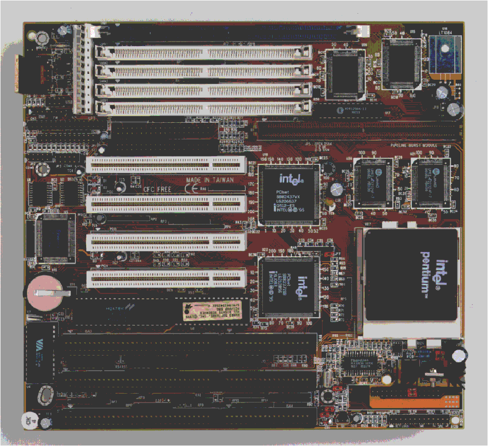
However, if you look at the board shots above, the second one is by me and taken from a working PC (presumably) with warranty stickers from the same OEM builder, J1/J2 Vcore is almost a sure bet.

J1/J2: Vcore
Open: 2.8V
Short: 3.3V

As for JP9, it's the same for both Pentium and MMX CPUs, I would presume the 2-3, 4-5 setting is 66MHz, and that translates into FS1 0, FS 1 as per the table you linked:

file.php?id=16496

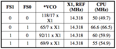
That means FSB is actually related to J9, and the correct FSB settings should be:

JP9: FSB
1-2 4-5 55 MHz
1-2 5-6 60 MHz
2-3 4-5 66 MHz
2-3 5-6 50 MHz

As for JP7/JP8, they have to be multiplier settings then.

JP7/JP8: Multiplier
JP7 JP8
1-2 1-2 2.5x
1-2 2-3 ??x
2-3 1-2 ??x (Judging by the other photo of this board online, a multilied that a P54C would use at 66MHz, most probably 1.5x as Taken boards don't seem to have 2x for Intel CPUs if TH99 is to go by..)
2-3 2-3 ??x

Retronautics: A digital gallery of my retro computers, hardware and projects.

Reply 7 of 7, by appiah4

User metadata
Rank l33t++
Rank
l33t++

Right, so I used this board in my P133 build and got around to testing its jumpers. Leaving this here in case anyone needs it in the future:

J1/J2: Vcore (as guessed)

Pinout for J1/J2
2 2

1 1
^ ^

Open: 2.8V
2 2

1 1
^ ^

Short: 3.3V
X X
| |
X X
^ ^

JP9 controls the FSB.

Pinout for JP9:
2 4 6
1 3 5
^

JP9: 50MHz FSB
2 X-X
1 X-X
^

JP9: 55MHz FSB
X-X 6
X-X 5
^

JP9: 60MHz FSB
X-X 6
1 X-X
^

JP9: 66MHz FSB
2 X-X
X-X 5

The board has no multiplier setup; it runs with what the CPU reports apparently.

Contrary to my hypothesis, JP7 and JP8 appear to have nothing to do with the multiplier. The board refuses to boot at 2-3 for me, but the only other photo of this board on the net has it on 2-3 so make of that what you will.

JP8 on 1-2 or 2-3 had no effect for me, but it might be CMOS clear (it did not occur to me to try the jumper with the power disconnected.)

Retronautics: A digital gallery of my retro computers, hardware and projects.