First post, by TheMobRules
WARNING: long post ahead! 😁
I've had an ASUS VL/I-486SV2G REV. 1.8 motherboard for a while, and after reading a couple of threads here I realized it was possible to convert it to the X4 version that supports lower voltage CPUs. Also, I noticed that most of the official and unofficial information about jumper settings refer to revisions 2.x of the board, which have significant differences to 1.x (in fact, I don't know if user manuals for revisions 1.x exist).
So, I figured it would be useful to have a comprehensive guide on how to do the mod for revision 1.8 as well as a detailed description of what each jumper does. My main sources of information were these two great threads:
Conversion guide for rev. 2.0, which includes many useful details, especially regarding voltage detection
Conversion guide for rev. 1.7, very similar to my 1.8 but does not do voltage detection and I noticed several differences in the jumpers
And also Jan Steunebrink's 5x86 upgrade page, which was extremely helpful when trying to determine what each jumper does with regards to L1 WB cache, VOLDET and clock multiplier.
So let's get started!
Components required
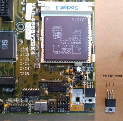
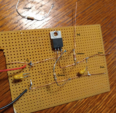
Here's an image of the board before the mod, with the locations where the new components will go, highlighted in color:
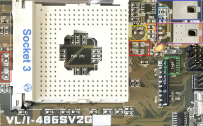
List of components:
- LT1085CT or equivalent adjustable voltage regulator [PURPLE]
- N-channel power MOSFET [BLUE], I used a STP16NF06L as suggested by user d0pefish in his 2.0 conversion
- 2 x 10uf 16V and 2 x 1uf 16V tantalum capacitors [RED]
- 330uf 16V electrolytic capacitor [YELLOW]
- 7407 hex buffer [GREEN]
- Two jumper wires to remove [LIGHT BLUE] and one to add [ORANGE]
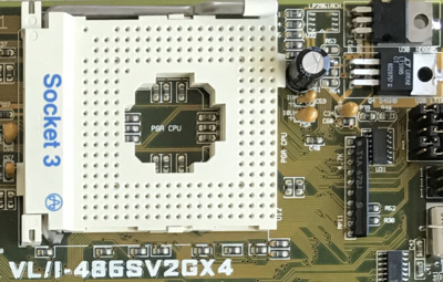
This is how it looks after adding the components (don't forget to remove the sticker to reveal the full name! 😎 ) :
Voltage detection
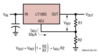
An output of the 7407 is connected to the MOSFET gate, while the drain is connected to +5V and the source is connected to the regulator output.
To enable CPU voltage detection, place a jumper cap over pins 4-5 of JP20. This will connect the VOLDET pin of the CPU to the corresponding input of the 7407, so a lower voltage CPU such as DX4 or 5x86 which ground VOLDET internally will use the 3.4V regulator output, while 5V CPUs will cause the regulator output to be shorted to +5V.
Leaving this jumper cap off will provide a fixed +5V to the CPU.
Write-back L1 cache
For some reason ASUS only provided L1 WB settings for 2.x boards, but placing jumper caps over the following pins will enable it on 1.8 (make sure to have the latest BIOS!):
- JP16 pins 1-2 (this connects the WB/WT# pin of the CPU to a pull-up resistor)
- JP17 pins 2-3 (this connects the W/R# output to the INV input of the CPU)
- JP18 pins 2-3 (this connects the HITM# input of the chipset to the HITM# output of the CPU)
- Finally, set both JP5 and JP6 to 1-2 for the proper L1 WB trap setting of the chipset
For WT L1, just leave the JP16, 17 and 18 jumpers off and set JP5 to 1-2 and JP6 to 2-3.
Clock multiplier
For CPUs that support the CLKMUL signal (such as DX4 and 5x86), the multiplier is controlled by pins 4, 5 & 6 of JP17:
- Leaving these 3 pins unconnected will cause CLKMUL to float, which sets the default 3x multiplier
- Placing a cap over pins 5-6 drives CLKMUL low, this sets the multiplier to 2x (4x for the AMD 5x86)
- Placing a cap over pins 4-5 connects CLKMUL to the BREQ pin, this should set 2.5x if the CPU supports it (untested)
Other jumper settings
- To enable power management on CPUs that support it, set JP16 3-4 (SRESET) and 5-6 (SMI ACT), as well as JP18 4-5 (SMI)
- For CPUs without NPU (SX) set JP19 to 2-3, the default is 1-2 for DX type
- Be sure to set JP20 to 2-3, setting it to 1-2 apparently connects the CACHE# output of the CPU to the corresponding chipset input for L1 WB, but doing so causes the system to hang during POST, so it looks like the CACHE# line is not used by the chipset on this board revision (also, it's not mandatory for L1 WB implementation according to Steunebrink)
Well, I hope this is a good source of info for owners of the 1.8 revision of this great board, as it was frustrating to me that pretty much all documentation I could find was on 2.x!