Great, so it was down to /MEMR signal. So from the bottom this time:
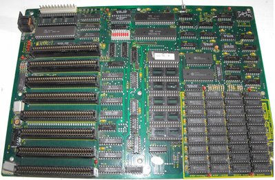
The schematic has a small error in U50 - pin 6 should be tied to VCC, not GND. Originally on IBM this was connected to /RESET line but here appears unused.
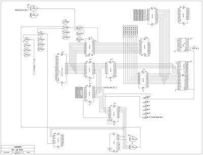
As for U37 and U43 - I think it would be easiest to try and explain this mobo as a set of functional blocks. Now actually the IBM design makes a bit more sense here, so I'll go with it and then address the differences.
So there is the CPU - 8088, which is the 8-bit bus variant of 8086 that wasn't actually used much, even if technically it started the family tree. 8-bit bus is easier to manage on the PCB, especially in the XT days with all the '74 chips around, not a lot of integration so the signals have to go everywhere. And that in itself is also a problem, we tend to think of the busses as some sort of magical connection that "just works" - but there are imperfections of the technology used, the voltage swing is not actually reaching VCC in TTL systems, and doesn't go all the way to ground either. The more chip inputs you connect the worse the output performance that drives them.
The first issue is the 8088 CPU is NMOS tech and really bad at driving H level. Not at multi-MHz speeds anyway. And because Intel opted for standard 40-pin package that was popular, there aren't enough pins for both address and data lines, as well as other signals. So the CPU needs a few extra chips, at least one latch for the lower address byte (the '373), one bi-dir transciver capable of getting the data both in and out (the '245), and amplifiers for the high data lines ('244 or '373, since if you are latching the low byte, might as well latch everything if you can). All this, along with the clock generator and 8288, forms a "CPU block".
Then you have the mobo chips, interrupt controller, RAM, ROM, all the address and control decoding logic, etc. There's so many of them that you might actually need extra buffers - that's another batch of 373, 244 and 245 chips. A "mobo block" then.
And finally there's ISA, and since you insert various cards into the slots, you want the slots separated from the CPU bus as well. Both due to how many chips might be connected here if all slots are populated, and because a faulty card could kill an expensive mobo chip. With a buffer it'll most likely just damage the easy to source 74 chips. That would be "ISA block".
And then there is the cherry on top - the DMA can take over the whole system bus to transfer data between ISA, CPU and the mobo. This too has to be isolated by buffers/latches that can be tri-stated. So that when DMA is doing ISA to memory transfer, the CPU signals will not interfere. This is "DMA block", and is separate even though DMA controller is part of the mobo obviously.
So it's not always all signals in all directions but you have 20 address lines and 8 data lines and some control ones, that must be both amplified and switched between various blocks that might be in control of the busses at the time. With just '74 logic you end up with these loops as you called them. The signals aren't actually supposed to loop, but the copper has to be there to allow those inter-block connections. In this particular example you're probably missing some more connections to other buffer chips, so this looks like a perfect, but useless loop.
And as for differences to IBM, this mobo seems to have the BIOS ROM (and maybe some other things too) connected to the "ISA block" rather than "mobo block". This is fine, so long all the chips work.
Now, for the test: First, measure voltage on the CPU data pins - you should read all H. Then use a resistor to bring the data pins on the ISA slot to L (so, connect to GND) and check if the respective data pin on CPU also went L. Pay attention to the voltage levels, if you get a pin that's somehow different value than other ones (even if the state is correct), take a note of it.
If you get any problems on the CPU pins, then test the A side (pins 2-9) of the U58 instead to see which one of the '245 is causing problems.
Oh and check again that in this mobo state (with the resistors in the 8288 socket) the /OE (pin 22) on the BIOS ROM is L.
If everything seems to work then it could be a faulty CPU, 8288 or some glitch that only manifests at high swtiching speeds. That raises the difficulty bar but perhaps custom BIOS ROM tests will help find it.