VOGONS


First post, by kikipcs

User metadata
Rank Newbie
Rank
Newbie

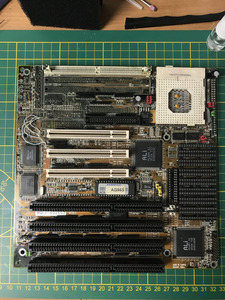
Been looking for a suitable 486 motherboard for my first personal 486 ever. Found it - MSI MS-4145. Manufactured in the 40th week of '95.
Very scarce information is available online on it - the most info I got on it was from Total Hardware '99. Seems everybody's talking about its older sis, the MS-4144.

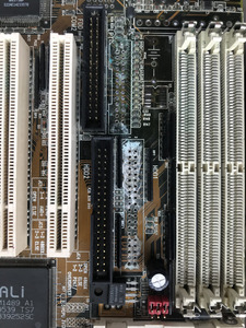
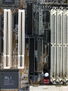
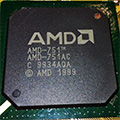
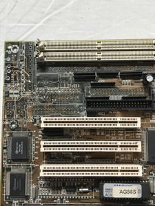
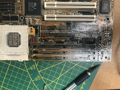
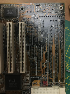
PCI + ISA, 8 full-size cache slots, the ALi 1489A1/SE chipset, 5V/3.3V adjustment, WinBIOS (woah), lots of possible CPU configs and more. Came with a Cx486DX2v66 CPU. Seems perfect for a 486 board.
Well, almost perfect. Cue the buzzkills:

1. The damage.jpg
Filename
1. The damage.jpg
File size
593.28 KiB
Views
1489 views
File license
GPL-2.0-or-later

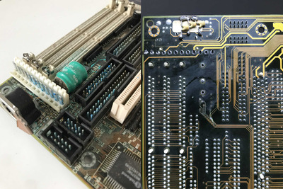
Initially I thought the leak was no biggie, but after treating the board with vinegar and brushes, the battery clapped right back at me.

top.JPG
Filename
top.JPG
File size
1.97 MiB
Views
1489 views
File license
GPL-2.0-or-later

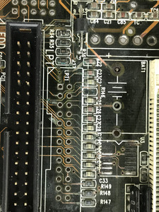
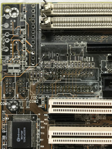
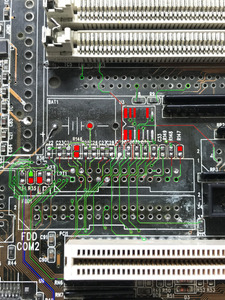
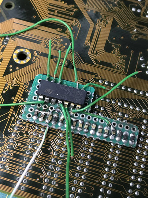
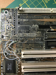
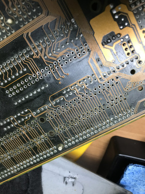
The gouge doesn't seem THAT bad - just need to solder two wires into vias. The leak damage, however, is much worse. While I can't spot any damage to the power rails, some of the traces have been completely eaten away. So, I started poking away, trying to get a clearer view and in the process "reconstructed" the wires.
Here's the result so far:

2. Traces.jpg
Filename
2. Traces.jpg
File size
701.42 KiB
Views
1489 views
File license
GPL-2.0-or-later

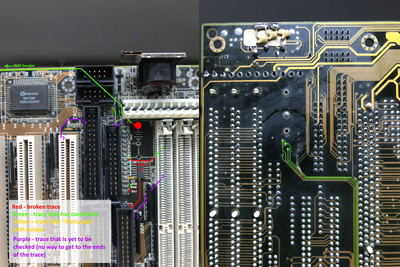
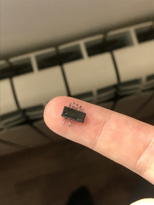
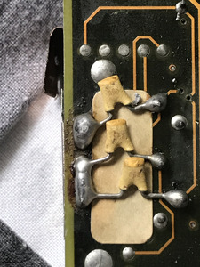
There's this mystery IC that has its markings eaten away. I've barely been able to read a part of the lower text: 74(?, looks like K or P?)04. No idea what this IC is, honestly, but there's a trace running under it, and at least one damaged trace on the underside leads to it.
The scrapes and exposed traces are my work; I've been poking around trying to guess the continuity on them.

I've already ordered a diagnostic POST card; perhaps it will come handy if/when we get to powering this thing up.
Now, I come asking for your help. This is my first foray into the magical land that is the 486 architecture. While it is a foray I've been yearning for for a long time, I have to take it slowly 'round here. Thus:

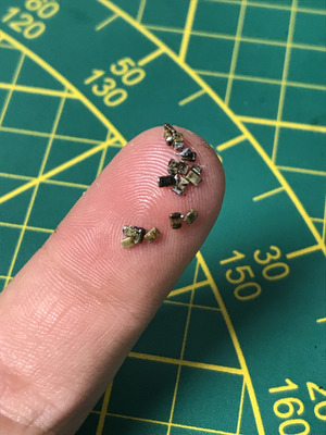
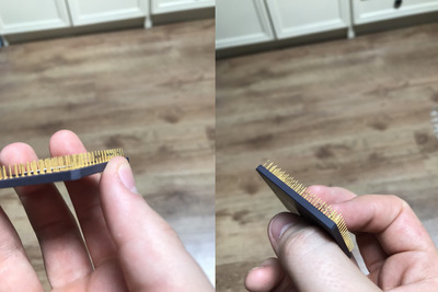
1) There are these odd dark marks on the CPU. Is this an indication of something bad?

3. CPU marks.jpg
Filename
3. CPU marks.jpg
File size
515.28 KiB
Views
1489 views
File license
GPL-2.0-or-later

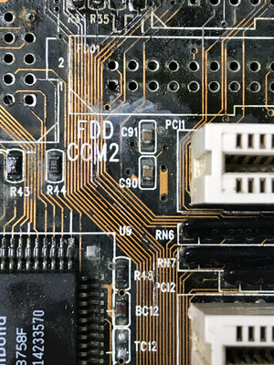
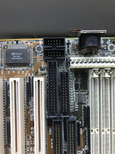
2) I am almost certain that I'm going to have to desolder the IDE, LPT COM1 and COM2 headers. But I haven't seen any of these that could be ordered online, so... is there any clean way to take these off in one piece or can I alternatively re-use the plastic shroud and just solder in a new header?

3) The memory slots might also need desoldering. Will the pins fall out when I desolder them?

4) The keyboard connector has this weird bodge. Can anyone guess what does it do?

4. DIN underside.JPG
Filename
4. DIN underside.JPG
File size
1021.67 KiB
Views
1489 views
File license
GPL-2.0-or-later

5) Is the damage THAT bad?

And before anyone suggests: No, I am not going to throw it away. Not yet. I've been looking for a board like this for more than a year now and I'm going to give it all I got. (aaaand there's several factors as to why I'm dead set on getting this thing fixed)
Plus, I'm not that keen to spend another $60 on a "gamble" board... 😁

Looking forward to your replies. Stay safe out there, y'all!

Reply 1 of 20, by evasive

User metadata
Rank Oldbie
Rank
Oldbie

1. that looks like the metal got quite hot. I hope I'm wrong .
2. I think that stuff is quite universal and you can buy any length of it with two rows of pins and cut it to size.
3. No
4. Debounce the input. I gues it was sensitive to HF something and this way you have less interference.
5. It is quite bad but not very extensive, you seem to have most in your view

The mystery IC is a TTL logic chips, I think it is a 6 port inverter basic designation 7404. Now the character in between defines the speed and switching characteristics. If I have to take a guess it is an F so 74F04 would be the actual part number. Seeing the condition of that it might need replacement too.

Reply 2 of 20, by evasive

User metadata
Rank Oldbie
Rank
Oldbie

I found scanned pages from the manual on archive.org

Attachments

  • Filename
    4145v11.zip
    File size
    1.84 MiB
    Downloads
    62 downloads
    File license
    Fair use/fair dealing exception

Reply 3 of 20, by kikipcs

User metadata
Rank Newbie
Rank
Newbie
evasive wrote on 2020-05-13, 18:00:
1. that looks like the metal got quite hot. I hope I'm wrong . 2. I think that stuff is quite universal and you can buy any leng […]
Show full quote

1. that looks like the metal got quite hot. I hope I'm wrong .
2. I think that stuff is quite universal and you can buy any length of it with two rows of pins and cut it to size.
3. No
4. Debounce the input. I gues it was sensitive to HF something and this way you have less interference.
5. It is quite bad but not very extensive, you seem to have most in your view

The mystery IC is a TTL logic chips, I think it is a 6 port inverter basic designation 7404. Now the character in between defines the speed and switching characteristics. If I have to take a guess it is an F so 74F04 would be the actual part number. Seeing the condition of that it might need replacement too.

Whew... that's a handful of information, but what lovely information! Thank you for your input! And thanks a lot for the manual - it'll come in handy to check all my jumpers, and I can already notice that the board does indeed support an external battery. Off to a good start, then!

The 74F04 does indeed look like my little IC. I've already looked some online; seems that there are some different revisions or something? For example, there's an 74LS04. I'll grab a magnifying glass and try to read the middle letter first.

The more I look at it, the more I'm certain that the power connector, the headers, 2 mem slots and possibly an ISA slot will have to be desoldered. I'm going to be taking off the DIN socket too, that's why I wanted to ask what that stuff was.

Well, I definitely will keep you updated.
Time to take this board to Desolderville.

Reply 4 of 20, by evasive

User metadata
Rank Oldbie
Rank
Oldbie

Oh the components on the DIN connector pins are ceramic capacitors. They are not polarized, just as long as you put them back on the same pins you should be fine.

Reply 5 of 20, by kikipcs

User metadata
Rank Newbie
Rank
Newbie

Update! Got better and worse news.

Desoldered the power connector, the DIN connector and some of the headers. It was a good idea to take them off.

Desoldered.JPG
Filename
Desoldered.JPG
File size
1.63 MiB
Views
1425 views
File license
GPL-2.0-or-later

About the mystery IC...
Can confirm it's a 74F04, but it was too far gone. Most of the pads came off right with it. The tinned pads are the only ones that emerged unscathed. Don't know how I'm gonna fix that yet - either I'm gonna glue some new pads or bodge wire the connections together and slap a SMD socket on it. I noticed that not all of the pads have a trace going out of them. Huh.

7404.JPG
Filename
7404.JPG
File size
726.72 KiB
Views
1425 views
File license
GPL-2.0-or-later

And I found out that the 7404 family has several members. Don't know which one should I replace it with - 74F04 is hard to get (i would have to wait a loooooong time) but I'm considering 74HC04 or SN74F04D. I'm not THAT knowledgeable on general electronics, but I guess one of those will suffice, correct? I'm already comparing the ratings and the 74HC04 seems to have bigger headroom when it comes to voltage. Any help here much appreciated.

During cleaning, one of the SMD resistors fell off with its pads. They were completely green on the underside, so the battery acid must've gotten under it.
The resistor reads: 100, so I assume it's a 10 Ohm resistor, right? It (and the pads) are so small that I don't know if I'm going to be gluing new pads. I'm thinking of using a "normal" THT resistor of the same rating in place of it. Is it possible?

7404 closeup.JPG
Filename
7404 closeup.JPG
File size
1.51 MiB
Views
1425 views
File license
GPL-2.0-or-later

Most of the damage (to the traces) looks to have been done underneath the LPT header. I don't care about it (it's not like I'm going to use an old printer anytime soon) so I think I'll just jump some wires to the vias.

Cleaned.JPG
Filename
Cleaned.JPG
File size
1.78 MiB
Views
1425 views
File license
GPL-2.0-or-later

I'm also concerned about the battery trace. It goes straight to the JBAT header so I assume it may need this connection. I'll try and re-tin the eaten trace or jump a wire, too.

Other than that, everything looks better than I expected so far. Still gotta figure out where this non-existent trace near U3 goes. Tomorrow I'm gonna draw a diagram of all the broken connections and desolder the RAM and more headers if need be.

Reply 6 of 20, by zyga64

User metadata
Rank Oldbie
Rank
Oldbie

SN74F04D is OK.
F - means fast, TTL levels of 0 and 1
HC - this is CMOS version, different voltage levels

1) VLSI SCAMP /286@20 /4M /CL-GD5422 /CMI8330
2) i420EX /486DX33 /16M /TGUI9440 /GUS+ALS100+MT32PI
3) i430FX /K6-2@400 /64M /Rage Pro PCI /ES1370+YMF718
4) i440BX /P!!!750 /256M /MX440 /SBLive!
5) iB75 /3470s /4G /HD7750 /HDA

Reply 7 of 20, by kikipcs

User metadata
Rank Newbie
Rank
Newbie
zyga64 wrote on 2020-05-14, 17:03:

SN74F04D is OK.
F - means fast, TTL levels of 0 and 1
HC - this is CMOS version, different voltage levels

Dzięki!
Couldn't find a proper explanation of what the different letters mean.

Reply 8 of 20, by zyga64

User metadata
Rank Oldbie
Rank
Oldbie
kikipcs wrote on 2020-05-14, 17:27:

Dzięki!
Couldn't find a proper explanation of what the different letters mean.

😀
https://en.wikipedia.org/wiki/7400-series_int … grated_circuits

Didn't noticed you're also Pole...
https://pl.wikipedia.org/wiki/Seria_7400
Najciemniej pod latarnią, hehe 😉

1) VLSI SCAMP /286@20 /4M /CL-GD5422 /CMI8330
2) i420EX /486DX33 /16M /TGUI9440 /GUS+ALS100+MT32PI
3) i430FX /K6-2@400 /64M /Rage Pro PCI /ES1370+YMF718
4) i440BX /P!!!750 /256M /MX440 /SBLive!
5) iB75 /3470s /4G /HD7750 /HDA

Reply 10 of 20, by quicknick

User metadata
Rank Oldbie
Rank
Oldbie

74HCT is also a possible replacement for 74F series; 74HC, not so much.

I'm tempted to say your board is in worse condition than the worst I've repaired, so I guess that makes it a perfect project for the current lockdown 😀

My approach is to desolder everything in the affected area, then use fine sandpaper to expose all the copper, tin the traces under plenty of flux, bridge any unwanted gap with copper wire of appropriate size and "double up" the corroded vias with short lengths from scrap IC pins. Thin copper wire can be used instead of the missing pads.

Your SMD resistors near the "epicenter" look particularly bad, I think you should replace them.

The marks on your CPU's pins look strange. Could be burn marks, if the board was powered with the CPU in a wrong orientation. But more likely the corrosion already reached the socket - you should remove the top piece (the one that slides when you move the lever) and check underneath.

Reply 11 of 20, by evasive

User metadata
Rank Oldbie
Rank
Oldbie

Could be burn marks, if the board was powered with the CPU in a wrong orientation. But more likely the corrosion already reached the socket - you should remove the top piece (the one that slides when you move the lever) and check underneath.

Oh I didn't even think of the second option. Really "pick your poison" here. As for not all the pins on the 74F04 being connected, you have separate 6 inverters in there each with one input, one output, not all of them need to be in use.

Reply 12 of 20, by kikipcs

User metadata
Rank Newbie
Rank
Newbie
quicknick wrote on 2020-05-14, 20:36:

74HCT is also a possible replacement for 74F series; 74HC, not so much.

Well... it really is black magic to me; only thing I can do is compare the ratings and they indeed seem almost identical, except the 74HCT04 has slower timing and slightly different H/L output voltage. I hope it doesn't pose much of a problem; I'll order the HCT and if it doesn't work like it should I'll try to source the F version.

I'm tempted to say your board is in worse condition than the worst I've repaired, so I guess that makes it a perfect project for the current lockdown 😀

My approach is to desolder everything in the affected area, then use fine sandpaper to expose all the copper, tin the traces under plenty of flux, bridge any unwanted gap with copper wire of appropriate size and "double up" the corroded vias with short lengths from scrap IC pins. Thin copper wire can be used instead of the missing pads.

Well, I've got time, patience, and some money to spend on it; why not try to get it fixed? 😉

I think I'm still gonna desolder more stuff, but I'm not going to bother with tiny traces that have been half-eaten already; I'm thinking of just running a wire on the entire length. Luckily the most damage is near the LPT header, and I don't really care about using it anytime soon, so I needn't worry about having to solder the header on top of all the repair work. Leaves more room for wires.

Your SMD resistors near the "epicenter" look particularly bad, I think you should replace them.

Yeah... since one resistor already came off with its pads, it'd be safest to assume that the same fate awaits the rest. I have no idea on how to fix this yet. though.

The marks on your CPU's pins look strange. Could be burn marks, if the board was powered with the CPU in a wrong orientation. But more likely the corrosion already reached the socket - you should remove the top piece (the one that slides when you move the lever) and check underneath.

The soldered pins (and the open vias) on the underside look pristine. I'm going to err on the side of caution and try to take off the socket soon.
The socket and the CPU themselves have black marker markings on them. Possibly to help align the CPU correctly for the past user of this board? Could be that he didn't heed his own advice...
The marks come off with a bit of friciton (i.e. a fingernail)

evasive wrote on 2020-05-14, 21:20:

Oh I didn't even think of the second option. Really "pick your poison" here. As for not all the pins on the 74F04 being connected, you have separate 6 inverters in there each with one input, one output, not all of them need to be in use.

Makes sense as to why some legs weren't connected to anywhere on the board - thank you! That means I don't have to worry about affixing the unused legs to the motherboard.

Reply 13 of 20, by kikipcs

User metadata
Rank Newbie
Rank
Newbie

Well, got more stuff desoldered. The old, oxidized solder was SUCH a hassle...

IMG_4157.JPG
Filename
IMG_4157.JPG
File size
1.96 MiB
Views
1284 views
File license
GPL-2.0-or-later

Luckily (or not) only 5 pads came off of the resistors - I expected more. The rest is happily nestled in place. There's a lot more damage to the traces, though - most of the LPT header's vias have no connection to them, and most of the traces going to the "resistor row" are also eaten. The X-Acto knife is a pretty good tool at that. Already tried establishing a map of known good/bad connections and gave myself a go at re-tinning the traces, with questionable result. Here's a close-up:

IMG_4159.JPG
Filename
IMG_4159.JPG
File size
1.91 MiB
Views
1284 views
File license
GPL-2.0-or-later

Bought some parts - new headers, 2x 74HCT04 in the SMD form, and a 74HCT04 in a DIP form.

Repairing the traces seems like a towering task, though, so I came up with an idea: why not try re-doing the 7404->resistors->LPT connections on a breadboard, and then connect the breadboard to the motherboard? Seems like a good idea... on paper. What do you think? 😉

Last edited by kikipcs on 2021-12-29, 00:30. Edited 1 time in total.

Reply 14 of 20, by evasive

User metadata
Rank Oldbie
Rank
Oldbie

For that section it might work, for the stuff around your memory slots, not that much. It looks like you need to remove at least one more memory slot because the fluid went under.

Reply 15 of 20, by kikipcs

User metadata
Rank Newbie
Rank
Newbie
evasive wrote on 2020-05-22, 14:18:

For that section it might work, for the stuff around your memory slots, not that much. It looks like you need to remove at least one more memory slot because the fluid went under.

Mhm, I'm only thinking about the chip and resistor row as they're closely related. The rest I can do with some simple wires.

For the time being, I still have to establish a map of known connections and draw up a project for the breadboard - looks like a fun weekend... 😉

Reply 16 of 20, by kikipcs

User metadata
Rank Newbie
Rank
Newbie

Update, sort of.

Didn't have enough time to work on the board - y'know, life gets in the way.

Kinda shifted my focus on the project; hardly think that I'm going to use it for a build due to increasing concerns for the stability if I get this thing repaired. For now, all that matters is getting it to boot.

Here's where I'm at with this board currently:

1) Lots of time spent on diagnosing connections. Every single (99% sure) damaged connection has been written down and mapped out.

Connections mapped.jpg
Filename
Connections mapped.jpg
File size
1.26 MiB
Views
1234 views
File license
GPL-2.0-or-later

2) Some of the pads/traces/vias where the corrosion happened are wayyyyy too far gone to spend time trying to connect stuff to it. I mapped out almost every single connection and am able to skip a lot of these broken traces with some kynar wire, luckily.

3) Some of the circuit (the resistor/MLCC cap "row" and the 7404 pads) will have to be breadboarded. Upon practising a bit with a dummy breadboard on a scrap board I think this is a pretty viable solution for the corrosion damage.

3) I collected most of the parts - replacement connectors, pin headers, the 7404 IC, battery header, internal speaker, bits and bobs.

The biggest issue for now is this row of SMD resistors and MLCC caps. I can't trust them enough to place them back into the circuit - the solder does not want to stick to them, despite countless attempts of cleaning and sanding the tiny suckers.
I tried to hold back as much as I could, but in the end - I need to replace them. Thing is, I have no idea what specs they are, so I can't buy replacements.
I even contacted MSI, hoping they'd provide me with schematics or tell the values. Long shot, I know, didn't hurt to try, but didn't work either.

Now, I'm no electronics engineer, but I do have some clues - they are 0805 caps, and one end, they either connect to the now-gone 3.6V battery or through a via to the ground plane, and on the other end - to the LPT port. I read up on the subject, browsed a lot of "broken off SMD cap" posts on various forums, and they all lead me to believe that my caps are used for noise filtering or decoupling. So they'd be of low value, like 0.1uF or something, maybe. But I still have to guess the correct voltage. If I had an LCR meter or an oscilloscope, that would help greatly... so I'm still reading up trying to confirm at least some more guesstimates for those capacitors.

Either way, until I learn what values the caps are, I can't proceed much further with the board.

Reply 17 of 20, by zyga64

User metadata
Rank Oldbie
Rank
Oldbie

You can measure resistors and capacitors using cheap LCR-T4 or LCR-TC1 (I have this one) meter.
There are several revisions with or without case, with monochrome or color display, with 9V battery connector or with USB connector for charging.
But all are more or less based on the same design. Can be bought via ebay (cheaper but you have to wait longer) or via allegro.pl (more expensive).

Voltage doesn't matter in this case (max voltage on motherboard is 12V). All ceramic capacitors are typically above this value (100V or more ?).
Electrolytic capacitors (where voltage matters) are usually large enough to print its value on top of the case.

1) VLSI SCAMP /286@20 /4M /CL-GD5422 /CMI8330
2) i420EX /486DX33 /16M /TGUI9440 /GUS+ALS100+MT32PI
3) i430FX /K6-2@400 /64M /Rage Pro PCI /ES1370+YMF718
4) i440BX /P!!!750 /256M /MX440 /SBLive!
5) iB75 /3470s /4G /HD7750 /HDA

Reply 18 of 20, by kikipcs

User metadata
Rank Newbie
Rank
Newbie

Holy smokes, over a year has passed. About time I gave you an update on this dumpster fire. Project burnout, pandemic, lack of skills, other projects, all that made a wonderful cocktail to sip on during the meantime.

Thanks to feltel for his recent post on this same mobo. My interest in the project was reignited!

First off - to refer to my previous attempts, they were really awful. A small walk of shame for you - this is how the board looked as of recently:

IMG_0256.jpg
Filename
IMG_0256.jpg
File size
1.79 MiB
Views
881 views
File license
GPL-2.0-or-later

Yeah. And this is that board I mentioned:

IMG_0260.jpg
Filename
IMG_0260.jpg
File size
1.41 MiB
Views
881 views
File license
GPL-2.0-or-later

This is an asinine idea and the sole fact that I thought this would be a viable fix is, in hindsight, very amusing to me. Shame I wasn't able to save the 7404. The whole board idea may have worked IF I used a printed PCB, or a custom flex cable, or a SOP12 to THT/pad adapter board... no. Maybe some other time, for another dumb project.

IMG_0257.jpg
Filename
IMG_0257.jpg
File size
1.72 MiB
Views
881 views
File license
GPL-2.0-or-later

Same goes for here - what was I thinking? Spaghetti and silicone sealing thingamajig that was allegedly hobby-spec but this would most definitely leave me with torn traces (and it did, haha)

So the first order of things is reversing this hackjob and properly cleaning the board. Then desoldering more stuff, except this time I'm taking the time and scraping away the oxidized solder so as not to end up with damaged vias, anger etc.

But to be honest, I learned some stuff in the meantime regarding the board. I managed to get in contact with MSI themselves and while they didn't share the schematics or anything, they did tell me that the SMD caps are not necessary for the board to work, and that they (almost all, I know one looks different and probably is different but these are such small values ) have the values of 180pF, 10V+. That's what I ordered.
Though, as a matter of fact, a lot of the traces and components I could just as well skip altogether, granted that the ones that go to other circuits on the board are fixed. The damage covers mostly the battery, power, peripheral and (unused) keyboard controller circuits. Power is obviously necessary, battery is two traces that I don't think will be needed since I'm going to be using the external battery header; peripheral could be bypassed by an I/O card (which I could also use if I don't manage to fix the onboard stuffs, knock on wood); KBC I might consider if I find a schematic that will assure me that the integrated controller does not support a PS/2 mouse (and I am guessing it does, since Ultimate Retro has a bios that supports it. I have the non-PS2 BIOS so that'll be on the list later). Don't get me wrong - I will attempt to do it all, it's just that it won't be a huge loss if something will still be broken.

Furthermore, I'm no EE but it appears to me that at least in the damaged part of the board, the ground plane is the middle layer, and the bottom layer is the routing layer. So even if some ground via is rotten beyond salvage I could bodge it to other ground via, et cetera. Could.

The chipset's cool too - 486 FINALi, with EDO and FPM support. Don't see many boards with this exact chipset nowadays. Again, I don't see me using this board in any build due to stability... but we shall see about that. I have zealously been watching Necroware, NorthridgeFix, other electronics repair guys and they don't mention stability concerns at all. Oh well, we'll see.

I have what I need to know for now, and I'm giving it another shot. More later.

Reply 19 of 20, by kikipcs

User metadata
Rank Newbie
Rank
Newbie

As mentioned and expected I did tear those traces:

IMG_0268.jpg
Filename
IMG_0268.jpg
File size
1.02 MiB
Views
874 views
File license
GPL-2.0-or-later

Learning from my mistakes, literally.

IMG_0267.jpg
Filename
IMG_0267.jpg
File size
760.23 KiB
Views
874 views
File license
GPL-2.0-or-later

Those ex-capacitors either crumbled when desoldering from that lamentable breadboard, or were so crispy that there was no way of telling which one is which. Most of the terminals on those separated from the body of the capacitor. I know there is one bigger SMD cap that is also damaged... is there any way to solder such a cap without such a terminal?

IMG_0323.jpg
Filename
IMG_0323.jpg
File size
1.65 MiB
Views
874 views
File license
GPL-2.0-or-later

Started the grueling task of scratching off the oxidized solder surface of the pins I have to desolder. Took me a lot of time. But desoldering said components was even more infuriatingly daunting... thank heavens I was eagerly huffing the isopropyl alcohol fumes to make it easier. Obviously joking, but it was hell to desolder, because even if the solder is scratched off, the pins and vias still may be oxidized/corroded, hurray! Flux, fresh solder, pump, more fresh solder, pump again, get angry, flux and solder wick, wiggle the pins furiously, rinse, repeat. A steady hand and steadier mind, and I managed to remove the last memory slot, the other IDE header, and the resistor ladders:

IMG_0385.jpg
Filename
IMG_0385.jpg
File size
1.9 MiB
Views
874 views
File license
GPL-2.0-or-later

Pleasantly surprised that it looks very good under those components! I thought I'd only see more green gunk and disrupted connections.
You might see some traces were tinned - that's me carefully considering simply tinning some existing traces instead of using bodge wires. Next was cleaning, then I ran a solder wick with some flux and a wide iron tip set at a cooler temperature (oh, what a difference good tools make!) to slowly even out the solder bumps remaining on the pins, reflow some of the vias, and see what is still too oxidized to make solder stick to:

IMG_0387.jpg
Filename
IMG_0387.jpg
File size
1.68 MiB
Views
874 views
File license
GPL-2.0-or-later

I was also surprised when exposing some of the traces - many of them seemed broken but they might actually only need tinning! On the other hand some were damaged more and disintegrated when cleaning, but they would have done so anyway. I have a dead Pentium 4 board from which I'm thinking of cutting out pads and epoxying them to the silicon. I will try this, but I am also considering simply placing wires and directly connecting them to SMD resistors and caps, then gluing them to the silicon. By the way - thinking of covering the tinned traces with lacquer (as seen in that black blob near the PCI slot). I don't have and don't plan to have a soldermask, so if you have an opinion or experience to share on using, say, nail polish, please do.

The next part is going to be cleaning out the vias, more trace/via exposure, and I'm going to start thinking about running wires. Some of the vias are already almost completely gone, unfortunately, but most of those simply run to ground - and even then, they are in a good shape on the bottom of the board. Repairable.

This is, dare I say, empowering!