Intel486dx33 wrote on 2020-08-12, 09:14:
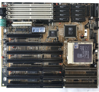
I have a gigabyte motherboard like this one. But i cant seem to get it to recognize any type of cache i have put in it.
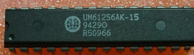
So I see this photo with “UM61265AK-15” cache.
Do you think this motherboard will only work with this name brand cache with these markings ?
If the cache chips are good, and JP1 and JP2 are set, the board should be able to recognized the cache. The vendor of cache chips does not matter at all, you can install all kinds of DIP28/DIP32 SRAMs that meet the required 15ns specification. Be careful with current offers of ISSI cache chips (espcecially 10ns ones) on ebay or chinese vendor sites - the common experience is that these chips have a quite high dead-on-arrival rate, and are most likely rebranded chips, as they are sold with datecodes and specifications that have been explicitly denied by ISSI insiders. The original chips might be factory rejects.
If none of your sets of cache chips work in this board, the board might be damaged. The last time I had a symptom like that, one of the address lines was scratched on the back side of the PCB. For a basic assurance test, check that
- All corresponding address pins of the cache sockets are connected.
- The data pins are connected between banks 0 and 1.
- All /CE, /OE, /WE pins are connected inside a single bank.
- All address pins (tag and data) are connected to at least one of the '373 chips next to the cache or 85c471 chip
- All data pins (tag) are connected to at least one of the '373 chips next to the cache or 85c471 chip
- All data pins (data) are connected to the 85c471 chip
Intel486dx33 wrote on 2020-08-12, 09:14:
What does AK and CK and Fk stand for in the markings ?
"K" is likely the code for the DIP case ("J" being the common code for SOJ), and "A" is the variant of the chip. If you want to check the datasheet for fine details, make sure you use the "UM61256A" datasheet, not the "UM61256" datasheet (they both exist).
Intel486dx33 wrote on 2020-08-12, 09:14:
Will 512kb cache chips work also ?
The manual of this mainbard specifies the use of 4 512kBit chips for 256KB cache (single bank) or 4 1024kBit chips for 512KB cache (single bank). The second bank uses the smaller DIP28 sockets that can only take 256kBit chip. See here for the manual: http://www.motherboards.org/files/manuals/47/486vs8a.pdf