VOGONS


First post, by mbertheau

User metadata
Rank Newbie
Rank
Newbie

Hi,

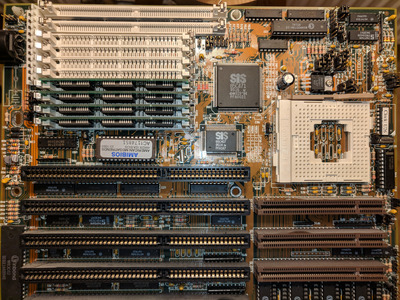
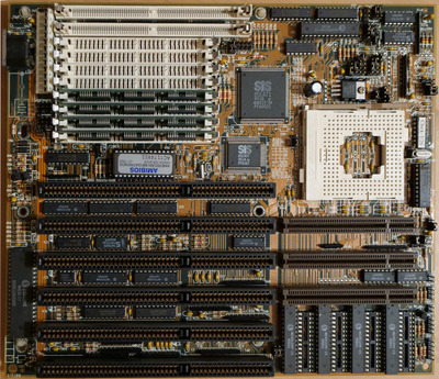
I've have a 486 board that, juding by the board layout and the chipset is a ABit AN4T R2 https://stason.org/TULARC/pc/motherboards/A/A … 4R2-AN4TR2.html

It doesn't boot correctly.

The barrel battery leaked a bit. I took the battery out and cleaned up the corrosion to the best of my abilities. There is now no battery connected.

The board has 4x4MB 30-pin SIMMs, a DX4-100 and 4 cache chips W24512AK-15.

The cache chips are 64K each according to the data sheet. The manual states that the board accepts either 4 32K or 4 128K chips. Is it indicative of a problem that there's 64K chips on the board?

I've made the following observations when booting the board with nothing connected except for the CPU, cache, RAM and speaker:

- no beeps from the speaker. Speaker works correctly - verified in another system.
- psu delivers 12 , -12 (+/- 0.5V), 5, -5 volts, measured at the motherboard connector
- ISA CLK on pin 20 ticks at 7.14 MHz
- There's activity on D0 and A0 on the BIOS ROM chip, verified with an oscilloscope. At first more complex patterns and then a short sequence repeated ad infinitum - I interpret that as a loop that the BIOS has decided to enter.
- the CPU gets warmer after a minute or two, so it's executing that endless loop maybe.

I don't have a POST card yet, that is something that I want to try next.

What other things can or should I try/test to diagnose this board further?

Thanks!

Reply 2 of 12, by Horun

User metadata
Rank l33t++
Rank
l33t++

Can you post a good picture of the board ?
Try a 5 volt 486DX or Dx2 just to eliminate the boards 3.3v vreg used for Dx4-100. Jp9 and Jp12 appear to set the voltage to either 5v or 3.3v
http://www.win3x.org/uh19/public/motherboard/ … c4071383153.pdf

Hate posting a reply and then have to edit it because it made no sense 😁 First computer was an IBM 3270 workstation with CGA monitor. Stuff: https://archive.org/details/@horun

Reply 3 of 12, by mbertheau

User metadata
Rank Newbie
Rank
Newbie
LewisRaz wrote on 2021-01-02, 17:59:

If you suspect the cache, try it with no cache. Also some boards do not like not having a CMOS battery.

I don't specifically suspect the cache, the observation just sounded odd to me. But I don't know enough to say whether a 64K module when a 32K module is expected is really odd or not.
Also the cache chips are fit quite tightly to the board, unlike the BIOS chip which has a space between the socket and the chip, which makes it easy to get the chip out. The cache chips don't have that. I'd like to try other things first.

I'll get a battery that fits on the external battery connector. That will take a few days though.

Horun wrote on 2021-01-02, 19:16:

Can you post a good picture of the board ?
Try a 5 volt 486DX or Dx2 just to eliminate the boards 3.3v vreg used for Dx4-100. Jp9 and Jp12 appear to set the voltage to either 5v or 3.3v
http://www.win3x.org/uh19/public/motherboard/ … c4071383153.pdf

I don't have a 5V 486 at home, but I'll get one and try that. Nice observation about J9 and J12 though. I'll see if I can measure the voltage supplied to the CPU directly to make sure it's 3.3V. Both J9 and J12 are in position 1-2 as far as I can tell.

When talking about jumper positions, is there a general rule about where pin 1 is? On this board it seems that pin 1 is always towards the ISA slot side of the board. But there was no obvious marker on the board for that.

Here's a picture of the board:

IMG_20210102_204537a.jpg
Filename
IMG_20210102_204537a.jpg
File size
1.83 MiB
Views
721 views
File license
Fair use/fair dealing exception

Reply 4 of 12, by Horun

User metadata
Rank l33t++
Rank
l33t++
mbertheau wrote on 2021-01-02, 20:09:

I don't have a 5V 486 at home, but I'll get one and try that. Nice observation about J9 and J12 though. I'll see if I can measure the voltage supplied to the CPU directly to make sure it's 3.3V. Both J9 and J12 are in position 1-2 as far as I can tell.
When talking about jumper positions, is there a general rule about where pin 1 is? On this board it seems that pin 1 is always towards the ISA slot side of the board. But there was no obvious marker on the board for that.
Here's a picture of the board:

Thanks ! On your board the #1 pin is signified by a box and the wider white on one side , look at JP12, JP60 (the one wired) and JP61 (the blank one) and you will see how pin 1 is marked.
Most boards there is no such "pin 1" is always toward left, right, ISa, etc as the design in diff areas would make that near impossible though jumpers in a group should be all the same orientation.

Hate posting a reply and then have to edit it because it made no sense 😁 First computer was an IBM 3270 workstation with CGA monitor. Stuff: https://archive.org/details/@horun

Reply 5 of 12, by mbertheau

User metadata
Rank Newbie
Rank
Newbie
Horun wrote on 2021-01-02, 20:24:

On your board the #1 pin is signified by a box and the wider white on one side , look at JP12, JP60 (the one wired) and JP61 (the blank one) and you will see how pin 1 is marked.
Most boards there is no such "pin 1" is always toward left, right, ISa, etc as the design in diff areas would make that near impossible though jumpers in a group should be all the same orientation.

I see, thanks! I'll pay attention to that.

Reply 6 of 12, by mbertheau

User metadata
Rank Newbie
Rank
Newbie
Horun wrote on 2021-01-02, 19:16:

Can you post a good picture of the board ?
Try a 5 volt 486DX or Dx2 just to eliminate the boards 3.3v vreg used for Dx4-100. Jp9 and Jp12 appear to set the voltage to either 5v or 3.3v
http://www.win3x.org/uh19/public/motherboard/ … c4071383153.pdf

Pin B7 on the socket is at 3.45V when the board has power, so that seems correct.

Reply 7 of 12, by mbertheau

User metadata
Rank Newbie
Rank
Newbie

I found it, and as often it's the simple things that I though I had covered. Two jumpers for the memory configuration were in the wrong place. The board boots fine now 😀

Thanks for all your help!

Reply 8 of 12, by Horun

User metadata
Rank l33t++
Rank
l33t++
mbertheau wrote on 2021-01-02, 21:40:

I found it, and as often it's the simple things that I though I had covered. Two jumpers for the memory configuration were in the wrong place. The board boots fine now 😀

Thanks for all your help!

Good job ! Yes is easy to not get a jumper set right when the board has many of them.
Can you take a picture of your boot up POST screen where it shows the BIOS ID string at the bottom and use NSSI or Uniflash to save and post the BIOS here ?
If you can do that we can add it to this BIOS topic: 80486 BIOS image collection or the Vogons Library http://www.vogonsdrivers.com/
and someone can add the parts to this: http://www.win3x.org/uh19/motherboard/search if needed, which is a creation of several talented Vogons members.

Hate posting a reply and then have to edit it because it made no sense 😁 First computer was an IBM 3270 workstation with CGA monitor. Stuff: https://archive.org/details/@horun

Reply 9 of 12, by mbertheau

User metadata
Rank Newbie
Rank
Newbie
Horun wrote on 2021-01-03, 01:45:

Can you take a picture of your boot up POST screen where it shows the BIOS ID string at the bottom and use NSSI or Uniflash to save and post the BIOS here ?
If you can do that we can add it to this BIOS topic: 80486 BIOS image collection or the Vogons Library http://www.vogonsdrivers.com/
and someone can add the parts to this: http://www.win3x.org/uh19/motherboard/search if needed, which is a creation of several talented Vogons members.

Will do, as soon as the PSU arrives, which suddenly stopped working correctly when I reassembled the PC. The crackling PC speaker sound gave it away. I hope all of the components survived. Measuring it again now with a multimeter and no load, the rails have the following voltage:

-12V is at -9.7V
+12V is at 11.05V
+5V is at 5.45V
-5V is at -5.14V

It did stop making a strange sound that it didn't make back when it was working fine, but those voltages still don't seem right.

Anyway, nice to know that the motherboard database people are around here! I'll definitely contribute any info I have.

I have two other PCs, a Pentium 200 MMX on a board with the Apollo VPX chipset according to HWINFO 6.12 with the string "08/14/97-VXPro+-USB-Ultr-2A5LDH09C-00", and a K6-2 400 on a Gigabyte GA-5AX with the string "06/17/1999-ALADDIN5-2A5KKG09C-00". Both have BIOSes on them that don't seem to be in the database yet, and lack photos. I can probably provide these. Where is the best place to put these infos?

Anyway, thanks!

Reply 10 of 12, by computerguy08

User metadata
Rank Member
Rank
Member
mbertheau wrote on 2021-01-03, 22:25:

Anyway, nice to know that the motherboard database people are around here! I'll definitely contribute any info I have.

I have two other PCs, a Pentium 200 MMX on a board with the Apollo VPX chipset according to HWINFO 6.12 with the string "08/14/97-VXPro+-USB-Ultr-2A5LDH09C-00", and a K6-2 400 on a Gigabyte GA-5AX with the string "06/17/1999-ALADDIN5-2A5KKG09C-00". Both have BIOSes on them that don't seem to be in the database yet, and lack photos. I can probably provide these. Where is the best place to put these infos?

Anyway, thanks!

You can put any info that you have in this thread, we'll add it to uh19.
Regarding the Abit board of yours, the photo cuts at the cache slots. If you could take a photo of the entire PCB, that would be appreciated.

And here is the page for that board (with BIOSes, manuals and the VRM mod): http://www.win3x.org/uh19/motherboard/show/73

Reply 11 of 12, by Deksor

User metadata
Rank l33t
Rank
l33t

That's true, but the vrm mod described was made by trying to figure out what would work best. There we have the "official" method 😀

Trying to identify old hardware ? Visit The retro web - Project's thread The Retro Web project - a stason.org/TH99 alternative

Reply 12 of 12, by mbertheau

User metadata
Rank Newbie
Rank
Newbie
computerguy08 wrote on 2021-01-04, 13:00:

Regarding the Abit board of yours, the photo cuts at the cache slots. If you could take a photo of the entire PCB, that would be appreciated.

Here's a complete picture of the board:

Mobo.jpg
Filename
Mobo.jpg
File size
1.7 MiB
Views
578 views
File license
Fair use/fair dealing exception