First post, by mkarcher
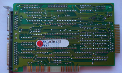
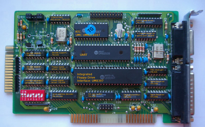
I happen to own a Turbo XT with this Multi I/O card I can not find in TH99:
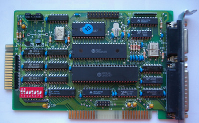
As I wanted to check for broken traces due to battery leakage, find out the switch settings and as I am interested in hardware reverse engineering in general, I reverse engineered that card. Let's start with the most interesting information:
This card is upgradeable. It has the RTC, the FDC, the game port and one serial port on the card, but it also has pin headers to mate with an extension board which provides another serial port and a parallel port. I don't own the extension board.
The switch settings are like this (effect of "OFF" / effect of "ON)
SW1-1: Game Port disable / enable
SW1-2: Clock disable / enable
SW1-3: Parallel port disable / enable
SW1-4: COM2 disable / enable
SW1-5: COM1 disable / enable
SW1-6: Parallel port base 278 ("LPT2") / 378 ("LPT1")
SW1-7: RTC base 240 / 340
SW1-8: unused
There also is a block of Jumpers:
JP1: 1-2 & 5-6 & 7-8 & 11-12: COM1 on base board, COM2 on extension board
JP1: 2-3 & 4-5 & 8-8 & 10-11: COM2 on base board, COM1 on extension board
The way the card works, SW1-5 controls COM1, which might be the port on the base board or the port on the expansion board, depending on jumper settings.
It is recommended to disable the parallel port and the COM port routed to the expansion board if the expansion board is not present, becasue the card still causes port conflicts on those addresses.
The game port is always at Port 201 (only), no mirrors in the 200-207 range.
The clock takes 32 ports, so 340-35F or 240-25F.
The parallel port is alwas at IRQ7, and the card claims the range 378-37F or 278-27F, although a parallel port only needs x78-x7A. As I don't have the expansion board, I can't tell you whether you get a mirror at x7C-x7E, or these ports are unused.
The floppy controller is fixed to the standard configuration 3F0-3F7, IRQ6, DMA2.
The serial ports are limited to 2F8-2FF/IRQ3 and 3F8-3FF/IRQ4. You cold swap the IRQs to obtain 2F8-2FF/IRQ4 and 3F8-3FF/IRQ3 by creative jumper settings, but there is absolutely no point in that in sane XT setups.
The remainder of the post is for the nerds among us:
All of the chips have datasheets available on common datasheet archive sites. The only special chip on that card is the address decoding PAL. I didn't try to desolder it and read the fuse mapping back (or brute-force it), but most of its behaviour is obvious:
U14 (PAL):1 A1 +5V 202 A2 RTCSW 193 A3 AEN 184 A4 /COMCS 175 A5 /LPTCS 166 A6 /RTCCS 157 A7 /GAMECS 148 A8 PPSW 139 A9 (GND) 1210 GND A0 11
- A0-A9, AEN are directly routed to the ISA pins with the same name.
- RTCSW and PPSW are inputs connected to the corresponding DIP switches. These pins are low when the switch is on.
- /COMCS is low on 2F8-2FF and 3F0 to 3FF (that's not a typo, /COMCS is also active on the FDC range)
- /LPTCS is low on 278-27F or 378-37F, depending on PPSW
- /RTCCS is low on 240-25F or 340-25F, depending on RTCSW
- /GAMECS is low on 201 only.
- Pin 12 is tied low in hardware. I have not tested how the PAL operates with Pin 12 tied high.
If you want to create a replica of the PAL to fix a copy of this board, you should have no problems creating equations for a replacement PAL given the behaviour description above. Keep in mind that the chip select lines only may only respond when valid port addresses may be on the bus, i.e. AEN is low. If AEN is high, address bits on the ISA bus indicate a memory address (DMA source/target), yet /IOW or /IOR will be asserted as part of the DMA cycle, so ignoring AEN yields false I/O decodes and strange behaviour of the card.
If you want to design a replacement expansion board for the card, you might be interested in the pinout of the expansion board connectors:
J1:1 D0 D1 132 D3 D2 143 D5 D4 154 D6 D7 165 COUT2 RESET 176 CCLK CIRQ 187 /IOW /IOR 198 /CCS /PCS 209 A2 NC 2110 A1 A0 2211 RX_D RSP_C 2312 OUT_C OUT_D 24J3:1 +5V +5V 62 +5V +5V 73 GND IRQ7 84 GND GND 95 +12V -12V 10
J3 doesn't need any documentation - all pins are directly connected to the ISA bus pins of the same name.
J2 is a bit more interesting
- D0 to D7 are connected to the local buffered copy of the ISA signals. They are forwarded to the ISA bus only if an enabled device on the card is selected. The direction depends on /IOR
- A0-A2, /IOR, /IOW and RESET are directly (unbuffered) connected to the ISA signals of the same name (RESET might be called RESETDRV, though)
- COUT2 is the interrupt driver enable pin for the external COM port. The interrupt driver is a 74LS125 on the main board. To create a PC-compatible COM port, this pin needs to be connected to the OUT2 pin of the secondary UART.
- CCLK is the clock (1.8432 MHz) for the secondary UART.
- CIRQ is the interrupt output pin of the secondaty UART. It's driven via the 74LS125 chip mentioned above to IRQ3 or IRQ4 (jumper selected).
- /CCS is the chip select signal for the secondary UART. It is decoded from /COMCS (PAL output) using A9, A3 by discrete TTL logic, and gated by SW1-4 or SW1-5. (jumper selected)
- /PCS is the chip select signal for the parallel port. It's the /LPTCS signal from the PAL gated by SW1-3.
- RX_D is connected to the input pin of a spare receiver in a XR1489 RS232 receiver chip on the base board. The "response control" chip of that receiver is is grounded, as is suggested for standard RS232 operation. The output of the receiver is connected to OUT_D.
- RSP_C is connected to the response control pin of another spare receiver in the same XR1489 chip. The input pin of that receiver is grounded. This configuration can also be used as RS232 receiver, but it provides a nonstandard (too high) impedance. I don't know whether this is a routing error on the card, or a feature. The output the receiver is connected to OUT_C.
To check for battery damage, the schematics of the "analog parts" near the battery might be handy:
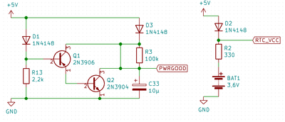
The supply for the RTC is straightforward: The battery is trickle-charged using D2 and R2 while the system is powered on. The RTC chip is supplied via D2. If the system is powered off, D2 inhibits the battery powering the system board, and the RTC chip is powered from the battery via R2. The current consumption of the RTC is so low that the resistor R2 does not matter.
To convert the card to lithium coin cell power, I replace R2 by a diode in opposite polarity of D2, and replace BAT1 by a coin cell holder.
The POWERGOOD signal is connected to the /POWERDOWN input of the RTC chip. The short over R3 is present on the card in the PCB traces. It's not a schematic mistake or a reverse engineering artifact due to a broken shorted component. On power-on, the charging of C33 delays /POWERDOWN deassertion, preventing the RTC from getting spuriously corrupted before power is stable. Due to R3 being shorted, the delay until C33 is charged is quite low, though. On power-down, interesting stuff happens. The first thing you need get straight is that Q1 is operated in Reverse Active Mode, mostly behaving as-if emitter and collector are swapped. As soon as +5V starts to drop out by around 1V, C33 turns on due to base being pulled low by R13 (and no longer being pulled up by D1), and the collector (being used as emitter) is pulled high by the remaining charge in C33. This turns on Q2 to quickly discharge C33, hoping that C33 is empty (putting the RTC in power-down mode, so it doesn't respond to bus cycles) before the system starts erratic behaviour due to VCC being low. The use of the reverse active mode in Q1 lowers its saturation voltage, so Q2 can get a stronger base drive even if C33 is already discharged quite deep.
Spoiler: No traces were broken on my card. Tracing out the analog circuit and measuring the integrity of all traces of it and traces going through it turned out to be unneeded.