First post, by lethal_guitar
I found a weird EGA card that seems to be some kind of hybrid:
It's from a German company called bit-design GmbH. I wasn't able to find much about this company online aside from an article (in German) from 1992: https://www.computerwoche.de/a/el-bildschirm- … technik,1134934.
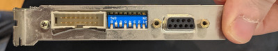
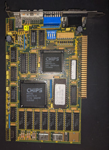
Seems that the company was making electroluminescent displays for the medical sector and for use in measuring equipment. The model that's mentioned in the article had a resolution of 560x400. I wonder if this card was able to drive that kind of display? Or maybe another EL based display, since it has "EL" in the name. It does have an unusual 16-pin connector and a regular 9-pin EGA/CGA connector. It also has tons of jumpers, and 12 dip switches in total. It's using a Chips & Technologies EGA chipset along with a bunch of other ICs which I assume are mostly related to the 16-pin connector.
I have tried this card in my 286 board, but didn't get a picture. I wasn't able to find any documentation on this thing, so it's going to be tricky to figure out the jumper & switch settings. I've started to try and see if I can figure out some of them by doing continuity testing, to see what's connected to the C&T chipset (the datasheet for that is fortunately easy to find). I have already figured out the following:
- J4 - switches IO address between 2xx (closed) or 3xx (open). It's directly connected to the IOADS pin on the chipset, so this one was obvious
- J8 - very likely switches between CGA compatibility and EGA mode. It connects pin 2 of the DB9 connector either to GND or to some other path that I haven't fully followed. But pin 2 is NC in CGA mode and Red 0 in EGA mode, so it seems fairly plausible that it would have that function.
I also found out that the bank of 4 dip switches is not connected to the C&T chipset directly, but switches 1 to 4 of the bank of 8 are. So maybe those 4 accept the same configuration that other C&T cards do, which usually have just one bank of 4 switches? The other dip switches are connected to some of the other ICs and to the "feature connector" pins of the C&T chipset, so my assumption so far is that they control the other video output's configuration.
For some of the other jumpers, I was able to find what they connect to, but couldn't really make sense of it yet:
- J7 can connect ADDR8 of the BIOS ROM chip either to +5v, or to ADDR14 on the C435 chip.
- With J5 and J6, it's possible to connect ADDR14 to either +5v or GND
- J12 connects one of the other ICs (SN74AS151N) to the FCOUT1 pin of the C436 chip
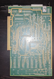
I've found data sheets for all of these ICs and I'm slowly working my way through finding all the connections. Basically doing a full on reverse engineering of the whole card now 😁 I'll keep working on this and share any new findings I have.