LocalBus wrote on 2022-01-29, 16:12:
You are definitely right about JP24 being the CMOS reset jumper. Most impressive how you are able to derive all this from the crude pictures.
It's mostly a case of taking the photos you've provided, using a tool to align them all (I just use GIMP), top and bottom, then seeing where the traces go. Each photo can be its own layer, and I can switch layers on and off. So if a trace on the top surface goes to a via then I can just turn off the top layer and pick up the via on the bottom surface. As far as I know motherboard designers try to keep inner layers for grounds and power planes, so most signal traces can be followed, unless they go under components.
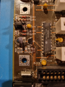
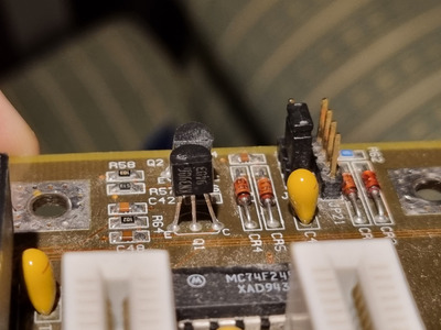
For instance, I can see that the thick trace from C48 goes to a via next to the ISA slot, but on the bottom layer it heads under the slot and out the other side, going to that 4069 chip. I can look up (or sometimes remember) that that's a bunch of NOT gates/inverters. It's right by the 32kHz crystal, which is used for the CMOS clock. So it's a fair guess that it's involved in generating the clock signal, which the battery will have to keep running, by feeding the output of a NOT gate back in to its own input via the crystal. At which point I could start looking for traces to confirm that. The trace disappears from the bottom layer, so I'd expect to see a thick trace emerging from underneath the 4096 and head in the direction of the 206.
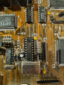
Will provide a more thorough update later, but I can say as much as R64 goes to OPTi 82C206 chipset. So this is what maintains the CMOS RAM voltage.
The side of R64 nearest Q1 should go to the Vcc pins of the 206 (pin 26 and 78). The side closest the board mounting hole should go to that PSRSTB# (pin 7). One thing worth doing is checking what the voltage is relative to ground on both sides of R64.
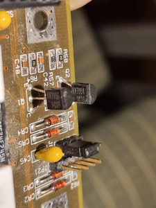
Now with JP24 in CMOS reset position I get sane diode mode readings from Q1 (PNP one). But the Q2 now reads 0.7V B-C, open C-B, 0.7V B-E and 1.9V E-B (should be open) in circuit, so this is my main culprit right now. I will desolder it and measure it out of circuit.
Don't forget that the Base of Q2 is between the voltage divider formed by R58 (to Ground?) and R57 (to +5V?). And that the Emitter of Q2 is probably connected directly to Ground. So the E-B junction is in parallel with R58 (10k). So your diode test will show a current flowing, but it's probably not through Q2.
C42 seems ok (no short). And the input to OPTi 82C206 is not shorted to ground.
What were you measuring when you found a short across C42 before?
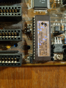
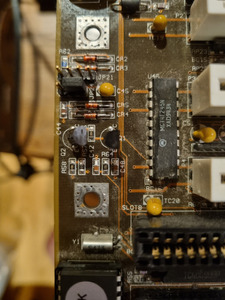
I have no idea about JP11 next to the BIOS ROM, maybe something about oscillator source?
Dunno. I'd start with guessing something involving programming voltage, maybe a size select?
Since you're getting some POST codes I'm figuring that accessing the BIOS is ok, so not too worried about that.
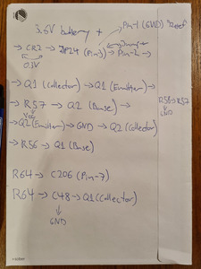
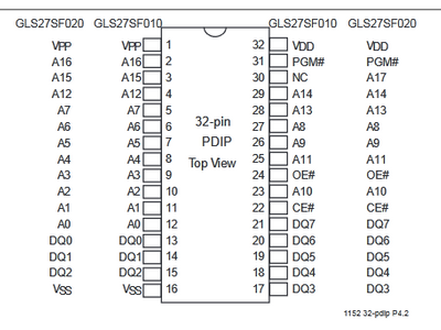
Quick skim of the notes look ok. It can make it clearer if you start drawing out symbols. I find it easier to grasp what connects to what by being able to see the lines connecting devices, and what any voltages between two points are by drawing arrows alongside them. You can take that schematic I posted earlier of the 206 charge circuit and you should be able to number all the components in that schematic with the component numbers from this board. E.g. R57 is the 51k resistor going from the base of the NPN transistor to Vcc.
For the moment, with the board off (but battery in place) I'd check the voltages (relative to ground) either side of R64, then measure them again with the board on.
Something possibly odd. Just skimming the Opti 206 datasheet and I can't see that it supports a low voltage supply for battery standby. The working voltage is given as 4.75 - 5.25V. So if R64 nearest Q1 is below that then that could cause problems, and the on board battery is around 3.6V?
Thinking back to your POST card results, one possible interpretation of the 0B fault was "CMOS checksum; video interface initialised". Maybe the BIOS is corrupted, or there's a problem with the video card? Hopefully Jan will be able to help with the BIOS once you get your TL-866.

