Reply 20 of 46, by maxtherabbit
Rank
l33t
- Rank
- l33t
Talimook
Talimook
stamasd wrote on 2022-01-20, 19:29:snufkin wrote on 2022-01-20, 18:44:Would you mind checking which pins on the Printer and COM headers are short to Ground? That way it might be possible to have a stab at working out the pinouts for those headers as well. If those are worked out then I think it just leaves the FDC and IDE headers, and they must surely (famous last words) follow the normal pinout.
the IDE, floppy, serial and parallel headers have pin 1 silkscreened on the board. The IDE ports work and have the normal pinout. The serial and parallel port headers have GND exactly where you expect them (just checked - i.e. COM pin 5, and LPT all even pins from 10 to 24), so I think safe to assume standard pinout too. The only one I haven't checked yet is the floppy header, and I have no reason to believe it's not standard.
Ah, I wanted to check, particularly the COM ports because there are two common standards, with the ground in different places, either in the middle or at the end.
1 2 1 63 4 2 7 1 2 3 4 55 6 or 3 8 -> 6 7 8 97 8 4 99 10 5 10
Given how you numbered the USB header (1-4 on one side, 5-8 on the other side), is your pin 5 at the end? Or are you numbering them as the IDE ports, with an even side and an odd side? Given how you describe the LPT header it sounds like you're numbering that as odd + even (so pin 26 is NC)?
stamasd wrote on 2022-01-20, 19:20:Garrett W wrote on 2022-01-20, 19:06:The 83MHz FSB bus however is another story, most devices won't be able to handle it. The PCI bus runs way too high at that speed courtesy of lacking a proper divider.
Like I mentioned above, this board's clock generator has the ability to run the PCI clock at a constant 32MHz independent of the FSB. It needs a slight hardware mod to enable that. I will get around to that, eventually. It's in the datasheet I posted a link to in the first post.
Frankly, what makes this motherboard interesting above others is that particular clock chip. With the option to run PCI async.
Hey, now that's pretty cool! Sorry, I completely missed this.
stamasd wrote on 2022-01-20, 19:20:Like I mentioned above, this board's clock generator has the ability to run the PCI clock at a constant 32MHz independent of the FSB.
I know some Intel chipsets don't support async, so it'll be interesting to know if that works when you can try it.
[edit: I've marked on the photos what I think are the pins you've found (obviously waiting for when you can check the PS/2). Do they look right?]
[edit: I've updated the COM port and removed the previous picture, hopefully that's now correct]
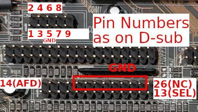
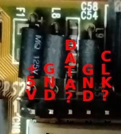
No, I used the COM header numbering as used here: https://pinoutguide.com/Motherboard/rs232_hea … er_pinout.shtml ( AT/EVEREX ) i.e. pin 5 is in the middle. Sorry for not being consistent. The LPT and USB above are correct, PS/2 awaits confirmation.
I/O, I/O,
It's off to disk I go,
With a bit and a byte
And a read and a write,
I/O, I/O
Garrett W wrote on 2022-01-20, 19:06:I don't see anything too unusual about this board. 75MHz and 83MHz for FSB were somewhat common, although obviously unsupported on the chipset. Not too shabby either way! If your CPU can take it (and that's almost certain for MMXs), the 75MHz FSB option is almost always guaranteed to work flawlessly. The slight increase on the PCI bus isn't enough to cause issues and in fact I've read magazines from that era that recommended it for light overclocking with a decent bump in performance. I'd use it, personally.
The 83MHz FSB bus however is another story, most devices won't be able to handle it. The PCI bus runs way too high at that speed courtesy of lacking a proper divider. I've heard tales of people using that bus setting and getting it stable with cherry picked hardware (including the motherboard I believe), but honestly I think it's way too much of a headache. 75MHz on the other hand is a nice, healthy boost in performance and generally trouble-free.
I've used six or seven different Asus P55T2P4s and TXP4s @ 500 MHz with K6-2+ CPUs over the last twenty years and have never had an issue with any of the hardware I've tried.
"I'd rather be rich than stupid" - Jack Handey
stamasd wrote on 2022-01-20, 14:13:Yes, but sometimes the BIOS string lies. I had to check, especially since TX didn't officially support those FSB settings. […]
Sphere478 wrote on 2022-01-20, 06:47:Lol it says 430tx at the bottom of post :pa
Yes, but sometimes the BIOS string lies. I had to check, especially since TX didn't officially support those FSB settings.
Sphere478 wrote on 2022-01-20, 06:47:Looks like you need a k6-2+ 570 for that beast 😀
I have one somewhere, need to find it. But the max multiplier I can set with this board is 3.5x, unless I misunderstand how multipliers work on k6-2. Guess I could use an utility like SetMul to set different multipliers.
(edit) oh wait, K6-2 interprets 2x as 6x, nice. So I could theoretically get to 83x6=499MHz. Assuming it likes the 83FSB, which it should. And that the other parts of the board are OK with it too. Worst case, I can mod the clock chip to force async PCI clock of 32MHz regardless of FSB, which it does support (see first post). A pull-down 10k resistor from pin 32 to ground should do that according to the datasheet.Sd performance on tx is pretty abysmal so if you have a couple 128mb simms laying around throw em in!
I plan to eventually, but for now I just did this quick testing with the 32MB which I had laying around.
May I introduce you to the tillamook pentium mmx 266?
I have one of those somewhere in a box too, have to find it. 😀
Isn't the Tillamook problematic in many ways though, as in L2 cache not working, having oddball I/O voltage (2.5V instead of 3.3V) etc?
The tillamook works fine on 3.3v I/O
And thanks to the efforts of people on this forum there are now fixes for the tillamook l2 and other issues. Tillamook 266MHz and working L2 cache?
Yes 2x=6x
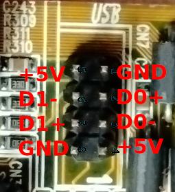
stamasd wrote on 2022-01-20, 17:40:Yeah I've tested both halves of the USB connector (one at a time using a standard USB bracket, because the second half has the w […]
Yeah I've tested both halves of the USB connector (one at a time using a standard USB bracket, because the second half has the wrong polarity if inserted normally) with a USB keyboard, and it's correct. I'll have to make an adapter to cross over the signals and make them match the pinout of the 2nd half of the connector on the USB bracket.
So using the numbering in the photo, the pinout for USB on this motherboard \ is:
1. GND
2. D1+
3. D1-
4. 5V
5. 5V
6. D2-
7. D2+
8. GNDwith pins 5-8 flipped 180 degrees from what they are on a modern USB header.
(update) I've actually managed to pull the wires from half of the USB bracket connector and reverse them WITHOUT destroying the connector completely. 😀 A bit of glue and tape, and now both ports on the USB bracket work correctly at the same time. Tested with the same USB keyboard.
Next time just use a razor blade to lift the tabs 🤣
stamasd wrote on 2022-01-20, 23:28:No, I used the COM header numbering as used here: https://pinoutguide.com/Motherboard/rs232_hea … er_pinout.shtml ( AT/EVEREX ) i.e. pin 5 is in the middle. Sorry for not being consistent. The LPT and USB above are correct, PS/2 awaits confirmation.
That's fine, it's not like they're consistent with their numbering. I think on most cases odds/evens makes most sense. I've updated the COM port picture so hopefully that's ok now until you can test out the PS/2 port.
[edit: just thought, when you get the PS/2 header, could you check on pins 2 and 4 if both of them are short to ground, or just one? I know you've measured 0V on both of them, but maybe only one is actually tied to ground.]
Sphere478 wrote on 2022-01-21, 05:46:Next time just use a razor blade to lift the tabs 🤣
I did - and it did not go as expected. 😀
I/O, I/O,
It's off to disk I go,
With a bit and a byte
And a read and a write,
I/O, I/O
For fun, I pulled today another CPU from my stash and tried to push it as much as possible in this board.
Cyrix 6x86L-PR200+GP, 2.9V, 150MHz (75x2)
booted fine and stable at default voltage and speed settings of course.
Since this board only allows me to specify multipliers of 2 and 3 for Cyrix, I dialed the FSB down and set the multiplier to 3:
50x3=150MHz, boots fine and stable
55x3=165MHz, same
60x3=180MHz, same
66x3=200MHz, 2.9V: POSTs but does not finish booting. Same happens if I push Vcore to 3.2 and 3.3V.
So this particular CPU likes at most 180MHz. It was completely stable at 60x3/2.9V when run through a series of benchmarks. And as expected, it scored higher than the P200MMX in integers but lower in floating point. 😀
(the BIOS recognizes it as "6x86L at 180MHz", no PR rating )
I/O, I/O,
It's off to disk I go,
With a bit and a byte
And a read and a write,
I/O, I/O
I found an undocumented jumper setting for this board. 😀
For Cyrix CPUs, jumpers JP1 and JP2 have only documented settings for multipliers of 2x and 3x (1-2, 2-3 and 1-2, 1-2 respectively) The other 2 combinations for JP1 and JP2 (2-3, 2-3 and 2-3, 1-2) are undefined for Cyrix CPUs.
So of course I had to try them. 😀
Bad news first: with JP1=2-3 and JP2=1-2, the motherboard does not POST at all at any FSB with a 6x86.
And good news: JP1=2-3, JP2=2-3 is read by the Cyrix 6x86 as 1x. 😀 So the CPU speed is the same as the FSB. This allowed me to underclock the 6x86 down to 50-83MHz. Yes, it is stable at 83FSB x1.
I/O, I/O,
It's off to disk I go,
With a bit and a byte
And a read and a write,
I/O, I/O
stamasd wrote on 2022-01-22, 14:48:I found an undocumented jumper setting for this board. :) […]
I found an undocumented jumper setting for this board. 😀
For Cyrix CPUs, jumpers JP1 and JP2 have only documented settings for multipliers of 2x and 3x (1-2, 2-3 and 1-2, 1-2 respectively) The other 2 combinations for JP1 and JP2 (2-3, 2-3 and 2-3, 1-2) are undefined for Cyrix CPUs.
So of course I had to try them. 😀
Bad news first: with JP1=2-3 and JP2=1-2, the motherboard does not POST at all at any FSB with a 6x86.
And good news: JP1=2-3, JP2=2-3 is read by the Cyrix 6x86 as 1x. 😀 So the CPU speed is the same as the FSB. This allowed me to underclock the 6x86 down to 50-83MHz. Yes, it is stable at 83FSB x1.
That’s wild, I had no idea that any socket5/7 cpus supported 1x
I had some fun recently with a 400gp figuring out it’s jumper settings
(Solved) Cyrix 400gp/366gp multiplier settings
stamasd wrote on 2022-01-20, 19:20:Garrett W wrote on 2022-01-20, 19:06:The 83MHz FSB bus however is another story, most devices won't be able to handle it. The PCI bus runs way too high at that speed courtesy of lacking a proper divider.
Like I mentioned above, this board's clock generator has the ability to run the PCI clock at a constant 32MHz independent of the FSB. It needs a slight hardware mod to enable that. I will get around to that, eventually. It's in the datasheet I posted a link to in the first post.
Frankly, what makes this motherboard interesting above others is that particular clock chip. With the option to run PCI async.
I have read the first pages of this thread with interest, in particular I find asynchronous PCI very interesting, I have no idea if you managed to get it to work, but in case it would be great, also because at high frequencies of FSB it would not cause problems for PCI cards, it would remain to be understood whether the controller also goes asynchronous or not.
Still on the subject of stability, I think it is normal that there may be some problems using the FSB 83, could it be due to the cache? Could the integrated chips in the MB be not fast enough? Have you tried disabling the L2 cache, to see if it works smoothly, obviously it will go a bit slower, but it would be interesting to understand exactly what causes the problem.
I created a page where I am collecting info on i430TX with FSB over 83MHz, a single motherboard starts with FSB 90, while an old ASUS MB with intel chipset has a non-working FSB over 100MHz, this however without modifying and replacing the quartz , it's here:
Re: Intel430 FSB settings beyond 83MHz (including overclocking?)
AMD 286-16 287-10 4MB HD 45MB VGA 256KB
AMD 386DX-40 Intel 387 8MB HD 81MB VGA 256KB
Cyrix 486DLC-40 IIT387-40 8MB VGA 512KB
AMD 5X86-133 16MB VGA VLB CL5428 2MB and many others
AMD K62+ 550 SOYO 5EMA+ and many others
AST Pentium Pro 200 MHz L2 256KB
FWIW, the Cyrix 200 was stable at 83FSB, multiplier 1x. The only card in the system was a Matrox G200 PCI.
I/O, I/O,
It's off to disk I go,
With a bit and a byte
And a read and a write,
I/O, I/O
So how low does it go? Down to 50MHz?
Yes it goes down to 50 MHz. It's weird to see on the POST screen "6x86L at 50MHz" but it works.
I/O, I/O,
It's off to disk I go,
With a bit and a byte
And a read and a write,
I/O, I/O
stamasd wrote on 2022-01-22, 14:48:I found an undocumented jumper setting for this board. :) […]
I found an undocumented jumper setting for this board. 😀
For Cyrix CPUs, jumpers JP1 and JP2 have only documented settings for multipliers of 2x and 3x (1-2, 2-3 and 1-2, 1-2 respectively) The other 2 combinations for JP1 and JP2 (2-3, 2-3 and 2-3, 1-2) are undefined for Cyrix CPUs.
So of course I had to try them. 😀
Bad news first: with JP1=2-3 and JP2=1-2, the motherboard does not POST at all at any FSB with a 6x86.
And good news: JP1=2-3, JP2=2-3 is read by the Cyrix 6x86 as 1x. 😀 So the CPU speed is the same as the FSB. This allowed me to underclock the 6x86 down to 50-83MHz. Yes, it is stable at 83FSB x1.
This is very interesting! I wonder which Cyrix CPUs can be set to 1x this way.
And nice to see this as a potential real purpose for these otherwise somewhat unremarkable CPU-curiosities 😜
So far I tested two 6x86 (one L and one non-L), specifically a 6x86-P166+GP and a 6x86L-P200+GP. It works for both. I also have an IBM 6x86L-166 which I haven't tested yet (because it needs a lot of work unbending pins) but I expect it to work also.
TBH I don't understand how it can possibly work. I'm going through the 6x86 datasheet at http://datasheets.chipdb.org/IBM/x86/6x86/6x86_ALL.pdf and this CPU only has one multiplier control pin: CLKMUL (page 3-7 in that sheet). It can only have 2 states: low or unconnected = multiplier 2x, and high = multiplier 3x. I have no idea how this board gets those CPUs to work at 1x.
I/O, I/O,
It's off to disk I go,
With a bit and a byte
And a read and a write,
I/O, I/O
Ah I think it starts making a little more sense. I was pointed to this thread from many years ago Subtle differences between Cyrix and IBM 6x86s where 1x for 6x86 was documented. The table in the first post refers to pins BF0, BF1 and BF2, which are not named so on the 6x86 according to the datasheet. But comparing the pinouts on the 6x86 datasheet ( http://datasheets.chipdb.org/IBM/x86/6x86/6x86_ALL.pdf page 5-1) and the Pentium MMX ( https://www.arl.wustl.edu/projects/archive/gi … X_Datasheet.pdf page 9) it appears that pins BF0 (location Y-33 in the latter) and BF1 (X-34) correspond in the 6x86 respectively to the pin CLKMUL and one "reserved" pin.
So if that "reserved" pin is indeed connected internally and influences the multiplier value, the findings above make more sense. And if the other combination of the 2 pin signals causes a 4x multiplier to be selected, it makes sense for the board not to POST in that case, because the minimum CPU speed would then be 50x4=200MHz, which I already know the CPUs I tested don't support (it didn't POST at 66x3 either).
I/O, I/O,
It's off to disk I go,
With a bit and a byte
And a read and a write,
I/O, I/O
Hmm yes and there is indeed a difference between the Cyrix-branded and the IBM-branded 6x86 chips. According to that table, the jumper combination that results in a 1x multiplier on Cyrix chips should give a 2x multiplier on IBM chips.
And practically, after unbending the pins on the IBM 6x86L-PR166+ and installing it with FSB=50 and JP1=JP2=2-3, it POSTS as a "6x86L-PR120+" which means it's running at 100MHz (not 50 as the Cyrix chip did). Still cool, but that means 50MHz is not achievable on this board with IBM CPUs, because there is no jumper to control BF2 and that would be the only method to get 1x for IBM.
I/O, I/O,
It's off to disk I go,
With a bit and a byte
And a read and a write,
I/O, I/O