VOGONS


First post, by eightbit

User metadata
Rank Newbie
Rank
Newbie

Hi everybody,

I was lucky enough to happen upon this board in great shape...although I have admittedly not tested it yet as I am waiting for an AT power supply to arrive 😀 You see, this will be the first 486 build for me in decades. I received the board with a 486DX-2/66 CPU, 4MB of memory and the board is population with some cache memory (more on that in a bit).

The board had the barrel battery which I promptly removed and thankfully no damage that I can see exists. I was researching breaking the charging circuit to add a CR-2032 to this and then I found this really useful link:

https://www.elhvb.com/webhq/models/486vlb3/sis486gh.txt.html

Apparently J1 is a provision for an external battery. Nothing marks that on the board clearly...it just says "J1". So good for this information! Now I do not have to modify the board and can add an external battery.

But then I was wondering if a jumper would need to be toggled to move from onboard battery to external....and I see this in the above linked documentation:

RC pin break switch enabled JP40 1-2
RC pin used for RC JP40 2-3

Is "RC pin" realtime clock? I cannot find any other reference to it anywhere online.

The other question I have is regarding the cache that is on this board. I cannot for the life of me find any reference to the part number. Each bank has a chip with these markings:

ST51256-20
9440 TAIWAN

All I can tell is that it is 20 ns...whatever it is. I guess I will find out eventually the capacity when I receive the PSU, but if anyone has any answer to the cache or the battery question please reply and I would be greatly appreciative!

Thank you!

Reply 1 of 19, by Deksor

User metadata
Rank l33t
Rank
l33t

I have this board
https://www.ultimateretro.net/en/motherboards/5549

I'm not sure how to change the battery jumpers but I suspect the one under the battery connector to be the one.

(Don't mind the schema, it doesn't match....)

As for the cache, is it soldered to the board ?
Because mine came with fake cache.
If not then it might be 256k of cache.

The fact it has fake cache isn't a big problem if you want to put some time into this, you can cut the fake chips from the board, desolder the legs put some sockets and put real cache chips.
It's not particularly hard even for a beginner, it's just time consuming because there are 32 x 9 joints to clear out and then to solder onto.

Trying to identify old hardware ? Visit The retro web - Project's thread The Retro Web project - a stason.org/TH99 alternative

Reply 2 of 19, by eightbit

User metadata
Rank Newbie
Rank
Newbie
Deksor wrote on 2022-03-02, 07:53:
I have this board https://www.ultimateretro.net/en/motherboards/5549 […]
Show full quote

I have this board
https://www.ultimateretro.net/en/motherboards/5549

I'm not sure how to change the battery jumpers but I suspect the one under the battery connector to be the one.

(Don't mind the schema, it doesn't match....)

As for the cache, is it soldered to the board ?
Because mine came with fake cache.
If not then it might be 256k of cache.

The fact it has fake cache isn't a big problem if you want to put some time into this, you can cut the fake chips from the board, desolder the legs put some sockets and put real cache chips.
It's not particularly hard even for a beginner, it's just time consuming because there are 32 x 9 joints to clear out and then to solder onto.

The jumper under the battery connector is clear CMOS.

The cache is real, it is socketed.

Reply 3 of 19, by eightbit

User metadata
Rank Newbie
Rank
Newbie

Well, received the PSU today and it is real cache, 256K installed, so each of these are 32K. Odd how I can find no reference to any of these chips however.

The external battery connector also works fine with no jumper needed to change. Just take the battery out and add an external. Easy!

As for the RC pin, that has something to do with power management as I see it referenced in that section of the BIOS.

Guess I answered my own questions, except for who makes that cache memory. If anyone ever finds out I would love to find out!

Reply 4 of 19, by Deksor

User metadata
Rank l33t
Rank
l33t

Can you tell me what's your bios (take a picture of the post screen)
Because I'm looking for all the bios version made for this board. If that's a bios we don't have, please dump it (you can do it via software, I'll give you a link)

Trying to identify old hardware ? Visit The retro web - Project's thread The Retro Web project - a stason.org/TH99 alternative

Reply 5 of 19, by tauro

User metadata
Rank Member
Rank
Member

I recently got the "SIS 486G 3.3/5V Rev: H". It's quite a fast board.

It has fake cache chips but the traces seem to be correct, though I'm not completely sure. The BIOS reports 256k cache... so maybe it doesn't have the right code to use a real cache? If I were to replace the fake cache chips, I should also replace the BIOS, right?

I replaced the fake cache chips on a different board once, and it made no difference. Furthermore, it worked for some time but then it just didn't post anymore.

Deksor wrote on 2022-03-03, 10:10:

Can you tell me what's your bios (take a picture of the post screen)
Because I'm looking for all the bios version made for this board. If that's a bios we don't have, please dump it (you can do it via software, I'll give you a link)

I could send you the BIOS rom if you are interested. I tried to contact the maintainer of theretroweb to send him this kind of stuff but he never got back to me.

This is the BIOS string "07/12/94-SIS-85C471B/E-2C4I9AD0-00" and the BIOS message is "AV_7542 VER. R08".

Anyway, here are some pictures. I cleaned up the battery leakage mess and replaced it with a CR2032 holder with a Schottky diode in series. So far it's working well.

Attachments

Reply 7 of 19, by tauro

User metadata
Rank Member
Rank
Member
Disruptor wrote on 2023-01-29, 05:52:

Can you run SpeedSys 4.78 on it (part of DOSBENCH suite), and post a picture of the cache chart (bottom right of the screen) please?

Sure. This is the fastest I could make it go with a DX2. I didn't do extensive testing and tweaking though.

Speedsys
CPU - 25.23
Mem. Bandwidth - 112.87 MB/s
L1 (8K) - 62.71 MB/s (62.62/63.57/61.94)
Mem. Throughput - 41.78 MB/s (31.90/63.57/29.88)

Cachechk
!! cache is 8KB 67.9 MB/s 15.4 ns/byte 194% 3.9 clks
Main memory speed 34.9 MB/s 30.1 ns/byte 100% [read] 7.7 clks
Effective RAM access time (read) is 120ns
Effective RAM access time (write) is 60ns

Attachments

Reply 9 of 19, by tauro

User metadata
Rank Member
Rank
Member
Disruptor wrote on 2023-01-29, 06:26:

In this SpeedSys chart there is definitively no L2 cache present or enabled.
Does the BIOS show an enabled cache in this configuration?

Yes, I'm quite sure that there is no L2 cache and that these chips are fake. I thought you wanted to see how fast the board performs.

The BIOS doesn't have an option to toggle the external cache on or off, only the internal cache. That's also suspicious. As I mentioned this is not the first board with fake cache that I encounter so I'm used to their shenanigans. As soon you boot you see "Cache Memory : 256K". It's hard coded. That's why I'm considering changing the BIOS if I replace the fake cache chips.

Here's the only reference I could find to these chips, from a Russian forum where they list fake cache chips.
https://www.phantom.sannata.org/viewtopic.php?t=25611

Reply 10 of 19, by Disruptor

User metadata
Rank Oldbie
Rank
Oldbie

Yes, the SpeedSys chart reveals a lot of things. (fake cache, misconfigured cache, ...)

But you can enable the hidden L2 option in your BIOS with modbin.
And you also can get rid of that 256 KB cache message with the same tool.

Reply 11 of 19, by tauro

User metadata
Rank Member
Rank
Member
Disruptor wrote on 2023-01-29, 07:08:

But you can enable the hidden L2 option in your BIOS with modbin.

That's a an interesting idea. I just checked and I can enable the option, but the L2 cache appears to be already set to Enabled by default. Maybe that means that real cache would work if I replace the fake chips but I'm not sure if this BIOS rom is "L2 cache ready". Heck, I'm not even sure if all the board traces are correct.

Disruptor wrote on 2023-01-29, 07:08:

And you also can get rid of that 256 KB cache message with the same tool.

How can I get rid of the "Cache Memory : 256K" message ? I didn't find it on modbin.

Attachments

Reply 12 of 19, by Deksor

User metadata
Rank l33t
Rank
l33t
tauro wrote on 2023-01-29, 07:36:

That's a an interesting idea. I just checked and I can enable the option, but the L2 cache appears to be already set to Enabled by default. Maybe that means that real cache would work if I replace the fake chips but I'm not sure if this BIOS rom is "L2 cache ready". Heck, I'm not even sure if all the board traces are correct.

It does work 😀

I used to own this board and just like you it had fake cache. I swapped the fake chips for real cache and it worked just fine. I didn't even need to mod the bios just like you

Trying to identify old hardware ? Visit The retro web - Project's thread The Retro Web project - a stason.org/TH99 alternative

Reply 13 of 19, by tauro

User metadata
Rank Member
Rank
Member
Deksor wrote on 2023-01-29, 09:24:
tauro wrote on 2023-01-29, 07:36:

That's a an interesting idea. I just checked and I can enable the option, but the L2 cache appears to be already set to Enabled by default. Maybe that means that real cache would work if I replace the fake chips but I'm not sure if this BIOS rom is "L2 cache ready". Heck, I'm not even sure if all the board traces are correct.

It does work 😀

I used to own this board and just like you it had fake cache. I swapped the fake chips for real cache and it worked just fine. I didn't even need to mod the bios just like you

Greetings!

It was a royal pain in the arse to remove all the fake chips. They don't have the same consistency as normal cache chips, they come apart easily and that hindered the process very very much.

Anyway, recently I received the sockets and before soldering them I found a few broken traces. After they were repaired... SUCCESS!

Was it worth it? Yeah! Because it works! ^^

I did not need to modify the bios, although the post screen still reports I have 256k, when in fact I'm doing some testing with 64k...

My advice for anyone willing to try this is try to avoid cutting the legs/pins of the fake cache chips, because then you need to remove them from the top side of the board and it's quite uncomfortable to work like that, since there are many components around and very little space and believe it or not, they don't come out easily. Had it been a regular cache chip or whatever other chip the process would have been much easier. I have desoldered entire 16-bit ISA slots that were easier to desolder than these disgraceful fake cache chips.

The DX2 66MHz, and 80MHz worked fine. But I can't get the DX4 to work , the same goes for the Am5x86.

Setting the gazillion jumpers in the correct position (indicated here the motherboard boots but after less than 60 seconds the screen goes blank (this doesn't happen if I open the BIOS options and leave it there). I tried setting the ram and cache to the lowest possible config and the behavior stays the same. After less than 60 seconds the screen goes blank. I also tried with a different ram stick.

I hope it's caused by a bad jumpers' config. I'm attaching a picture showing the way the motherboard looks and the current jumper placement.

Could you please share a working jumper config for a DX4 or Am5x86? Does the Cyrix 5x86 work with this motherboard?

Interesting fact: Setting the cache to write back (using the DX2) changes the speed of the main memory (ram) to half while the cache's speed remains the same.

Attachments

Reply 15 of 19, by Chkcpu

User metadata
Rank Member
Rank
Member
dj_pirtu wrote on 2023-02-13, 12:02:

Is the mobo same as this: QDI V4S471/G locks up with 1024kB of cache [Fixed! Nicer Award BIOS available!]

There's great BIOS for that.

@dj_pirtu
Although the QDI V4S471/G is a bit different than the Full Yes 486G 3.3/5V board, using a more recent SiS471 BIOS is a good idea and may actually work. Transplanting a BIOS from another board is not always successful, but with SiS471 boards this usually works fine. 😀

@tauro
In his thread, member GigAHerZ reports success with a 11/28/95 SiS471 BIOS on his QDI board. I’ve used the same up-to-date 11/28/95-SIS-85C471B/E/G-2C4I9G30-00 V3.06 BIOS from a Gemlight board successfully on several other SiS471 boards, like the Chicony CH-471B and the Full Yes 486G 3.3/5V! But I do adapt the default chipset register programming via Modbin to that of the original BIOS for each board, to maximize success.

For your FY-SiS486G board you can download this updated Rev J.1 BIOS here:

Filename
486G-J1.zip
File size
45.21 KiB
Downloads
39 downloads
File comment
FY-486G Rev J.1 BIOS
File license
Public domain

The user who tested this updated BIOS, reported that this 11/28/95 BIOS works fine on his FY-SiS486G board, running an Am5x86 at 4x 33 and L1 cache WB mode.

Being a late 1995 BIOS, it is free from the Year 2094 and 2GB Harddisk display limit bugs, and fully supports the Am5x86 and Cx5x86. It also displays the L2 cache size correctly.
Note that this BIOS shows the “L1 cache: WB/WT” option in the BIOS Setup only for the P24T and for Cyrix CPUs.
For the P24D (486DX2WB), Am486DX4WB and Am5x86, this 11/28/95 BIOS can detect if these CPUs are in WB mode and programs the chipset registers accordingly. It then hides the “L1 cache: WB/WT” option, because user interaction for this automatic function is not required.
So, you only have to find the correct jumpers for L1 WB mode and the BIOS takes care of the rest. 😉

Jan

CPU Identification utility
The Unofficial K6-2+ / K6-III+ page

Reply 16 of 19, by Deksor

User metadata
Rank l33t
Rank
l33t

@Chkcpu
thanks for the bios upload, I have added it here : https://theretroweb.com/motherboards/s/full-y … .3-5v#downloads 😀

Trying to identify old hardware ? Visit The retro web - Project's thread The Retro Web project - a stason.org/TH99 alternative

Reply 17 of 19, by Chkcpu

User metadata
Rank Member
Rank
Member

@Deksor
Thanks for putting the 486G_J1 BIOS up at The Retro Web.
Although the BIOS has been tested on an earlier revision of the Full Yes SiS 486G 3.3/5V board, I'm confident it will work on the Rev:G/H revisions as well.

@tauro
When you are able to try the 486G_J1 BIOS on your Rev:H board, please let us know how it works.

Jan

CPU Identification utility
The Unofficial K6-2+ / K6-III+ page

Reply 18 of 19, by tauro

User metadata
Rank Member
Rank
Member

Wow, so much information and help, thank you!

So, I got the intel DX4 working with the "DXL AM486DXL2" jumper configuration albeit JP10 needs to be in 1-2, otherwise it won't post. The voltage I can measure in the main transistor is about 3.5v (versus 3.8v with the previous DX4 jumper config, not that this is relevant but I leave it here for the record).

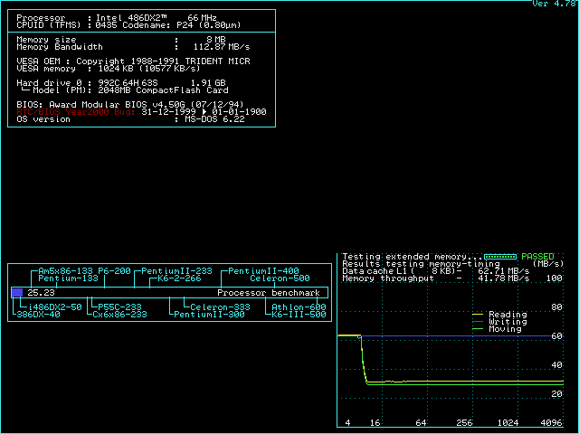
The motherboard works fine @100 MHz but I can't get the multiplier to go to x4 for the Am5x86. This CPU is always detected as an AmDX4 @100MHz.

Chkcpu wrote on 2023-02-13, 18:59:

@tauro
When you are able to try the 486G_J1 BIOS on your Rev:H board, please let us know how it works.

Jan, thank you very much for popping up. I came across your BIOS a few days ago (now I can't find the thread) and I was already giving it a try... "What can go wrong?" I thought. Well, nothing bad happened, but nothing good either, sadly. I still can't get the Am5x86 to work at x4. With the DXL2 config (JP10 1-2) it still works at x3 and is detected as an AmDX4 @100MHz. The DX4 jumper configuration still produces the same blank screen after less than 60 seconds after booting, so that's something to do with the sketchy jumper configs from the online manuals, I'm sure.

Chkcpu wrote on 2023-02-13, 14:22:

The user who tested this updated BIOS, reported that this 11/28/95 BIOS works fine on his FY-SiS486G board, running an Am5x86 at 4x 33 and L1 cache WB mode.

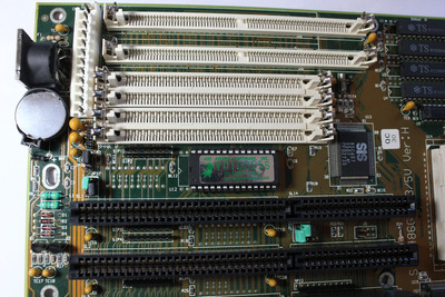
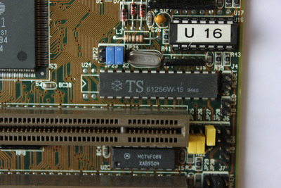
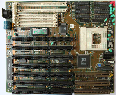
It would help a ton if any user with this board or a very similar one posted a picture of the working jumper configuration for an Am5x86 at x4!
🙏

The Am5x86 works at 40x3, but that's too slow, I usually run it at 160MHz or 150MHz. I tried 150MHz and... it works! But I need to add a wait state for the L2 cache and that kind of ruins all the meaning of running it at 150MHz and I also need to slow down the only VLB card I have... which isn't a great card either... so I think 160MHz would be the most adequate for this board, but that x4 multiplier... I can't find it.

Does anybody know which particular jumper block or blocks modify just the multiplier? This design is very unfriendly and there's contradicting information on the only 3 online references I found (the third one being this one). I tried some jumper configs (I'm still experimenting and I have some ideas) even the P24D config from here and it's always either a working x3 or x3 and the blank screen after some seconds. Interestingly, the good old DX2 worked at 66MHz, so assume it's possible to get a x4 since the Am5x86 is supposed to work at x4 with the x2 configuration... but still I haven't found a way to get it working at x4.

Chkcpu wrote on 2023-02-13, 14:22:

So, you only have to find the correct jumpers for L1 WB mode and the BIOS takes care of the rest. 😉

I would really like to know what are those jumpers... There are so many and so many possibilities. Having the option to chose between WB and WT is convenient. According to my tests on other motherboards some software performs better with WT, like Quake for example, not that I'm interested in it but it's nice to be able to tweak things.

Could you recommend me where to start to figure everything out?

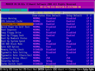
Something that is really important is that this BIOS doesn't let you change the ram speed (it only lets you use Faster) and that's very limiting for testing. I don't know if this is something done purposefully or if it's because of an incompatibility. I'll inspect it with modbin in the future. It would be interesting to compare the modded BIOS using the Am5x86 vs the stock BIOS, but I'm still limited by the x3 multiplier.

Reply 19 of 19, by Chkcpu

User metadata
Rank Member
Rank
Member

Hi tauro,

Yes, there is a lot of contradicting jumper information out there for this board.
But I agree that your issues should go away with the correct jumper settings.

I found another set of jumper settings for your SiS 486G 3.3/5V board at
https://www.elhvb.com/webhq/models/486vlb3/sis471g.txt.html
This set is the closest match I could find, looking at the picture of your Rev:H board, and it has jumper settings for the AMD Enhanced 486DX4-120 WB!

Before hunting for the x4 multiplier jumper, I would advice to test your Am5x86-133 with these Am486DX4-120 WB settings. The BIOS should indicate an Enhanced Am486DX4 at 120MHz and a utility like my CHKCPU tool should tell you that the L1 cache is in Write-Back mode.
Then try to boot from a floppy to test if the CPU-Chipset L1 cache WB interface works okay.

When this all works fine, you can use the "Clock Multiplier jumper" procedure from my Am5x86 article at http://www.steunebrink.info/amd5x86.htm
to find the x4 jumper.

Good hunting!
Jan

Edit: updated my website link

CPU Identification utility
The Unofficial K6-2+ / K6-III+ page