VOGONS


First post, by RussD

User metadata
Rank Newbie
Rank
Newbie

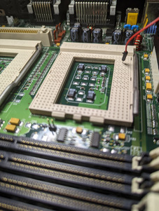
I received a Micronics W6-LI dual Pentium Pro motherboard from storage and wanted to get it up and running. I got it in a case with a power supply, video card, memory etc. And tried to boot it up. No beep, no video, nothing. Time to get down to the business of debugging the POST failure. I'll include the process I went through in this thread to debug the issue and get the board booting. And yes, the story does end with the board booting. Between waiting for tools/parts, and finding time to work on it, it took about 3 weeks. Rather than jump to the end, I'll post "updates" every couple of days or so. If people want to jump in and guess what the problem is as this goes along, you're free to do so.

PXL_20220629_180738743 (1).jpg
Filename
PXL_20220629_180738743 (1).jpg
File size
1.92 MiB
Views
1355 views
File license
Public domain

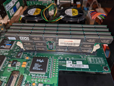
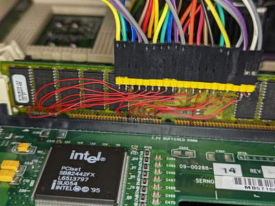
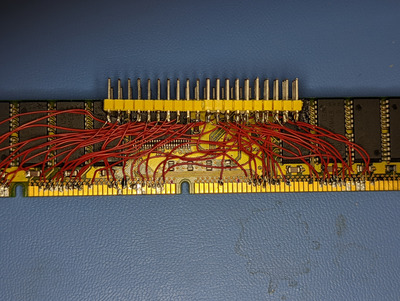
Anyway, the board came with some RAM, but I had ordered 1GB of RAM since it was only $35 for the set. Pressing the power button caused it to turn on and immediately off the first time, the second time it turned on and stayed on. But no beep, no video, etc. I began by taking out all the expansion cards, swapping back in the 128MB stick that it originally had with it. Tried again. No beep. I took out the second Pentium Pro and it's VRM. Still no beep. Checked the speaker connection, tried a different speaker. No beep. Swapped the second pentium pro into the slot of the first one. No beep.

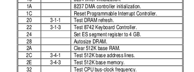
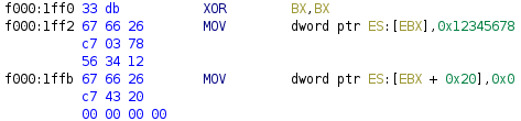
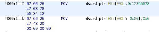
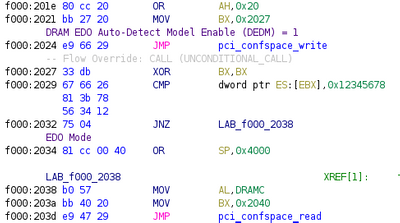
Okay, time to go a little more in depth. I grabbed a copy of the motherboard manual and verified each of the jumper settings. All correct. I next tried resetting the CMOS. No help. Checked the CMOS battery for good measure. I backed up a bit to the issue with the system initially not powering up. I left it off for a while, put all the cards back in and the second pentium pro and had the same issue again where the first time I pressed the power button, it powered on and immediately off, and the second time it powered on and stayed on. Maybe I'm dealing with a power supply issue? I don't have any others easily accessible so I put the system away for now, ordered a new EVGA 650W power supply and a cheap POST diagnostic card. Both will arrive in the next post.

Reply 1 of 25, by RussD

User metadata
Rank Newbie
Rank
Newbie

Ok, the POST diagnostics card and the power supply has arrived. Lets try them out.

First the new power supply. Press the power button, machine turns on for a half second and then off again. Pressing the power button again and again results in the same thing. Ugh. This is worse than with the old questionable power supply. Maybe there's a short somewhere? Lets repeat some debug steps from the old power supply starting with taking out the expansion cards. Oh, hey, now it works. Lets try one card at a time to find the faulty one...hrm...It's not one individual card, it's just if there are "enough" cards installed. There just doesn't seem to be enough omph on of the rails. Alright, lets take enough cards out for it to run, and then let it run for 15 minutes or so and check for hot spots. ... no hot spots. If I run it with all the expansion cards but without the second PPro and VRM, it also runs fine. Holding the VRM in my hand I notice it has an awful lot of big capacitors. 6000uF on the 5V rail, and 4000uF on the CPU voltage rail. I'm beginning to suspect that either newer power supplies are very good at ramping quickly thus causing massive inrush currents, are very sensitive to tripping due to large in-rush currents, or both. I'll leave the second pentium pro out for now and put that issue in the "later" column.

OK, the POST card. Looks a bit dodgy with some really sad documentation, but what are you going to do. Lets plug it in and turn things back on. Hey, things are happening, numbers are changing, huzzah. And it stops on 28. Lets check our codes:

gnome-shell-screenshot-4v3hdb.png
Filename
gnome-shell-screenshot-4v3hdb.png
File size
19.28 KiB
Views
1321 views
File license
Public domain

So it doesn't like the DRAM. Maybe these oversized ebay modules I got for a steal are a bit dodgy? Trying the memory module the motherboard came with...Nope same code. Try a different slot? Try with no module? Same code, same code. Clearly the BIOS is having some sort of problem communicating with the DRAM. Visual inspection of DRAM slot? Looks good. Well, maybe my ebay modules don't work with this board, and the module the board came with is bad. I can get a 32MB module on ebay for $10, seems like a decent thing to try next because I'm running out of ideas. Just gotta wait for it to arrive, hopefully the seller is quick about things.

Reply 2 of 25, by RussD

User metadata
Rank Newbie
Rank
Newbie

Hooray, the new memory module has arrived! Time to test. Swap it in, press the power button and watch the POST card for exciting news.....and.....nope. Very discouraging. There's clearly something wrong with the motherboard. I've examined both processors, they both look good and running with either leads to the same result. It seems unlikely that both are bad in the same way. There's no expansion cards in the system and I've tried with 3 different kinds of ram modules now. It must be the motherboard.

First basic easy test. Voltages. Power the board up and test the termination voltage rails and voltage rail used by the DRAM. All are fine.

Lets move next to a careful visual inspection. There must be a bent pin or a broken trace somewhere

PXL_20220630_135026126.jpg
Filename
PXL_20220630_135026126.jpg
File size
1.44 MiB
Views
1296 views
File license
Public domain
PXL_20220721_190529011.jpg
Filename
PXL_20220721_190529011.jpg
File size
957.51 KiB
Views
1296 views
File license
Public domain

I haven't noticed anything inspecting the board carefully top and bottom. Paying special attention to the area around the processor, the 440FX chipset, and the DRAM slot. This is not looking good. The desperation phase has officially begun. The DRAM socket only has 168 pins. If the BIOS is failing on the DRAM, there's a good chance there's a problem there...right? OK, lets pull out the multimeter, some datasheets, and get probing! The module I bought actually makes this a little easier as it has vias right above it's connector for both signals on the front and the back which make really easy probe points that my probe tip likes to rest on. Anyway, at this point a very important part of diagnostics is keeping good notes. So some 168 beeps later we have:

dram.jpg
Filename
dram.jpg
File size
287.48 KiB
Views
1296 views
File license
Public domain

Well that's just peachy, everything is just fine. Going to have to take a step back and figure out how to get some more detail on what is failing and why, because the POST code alone clearly isn't pushing me in the right direction. Need to gather some more information and come back at this from a different direction.

Reply 3 of 25, by RussD

User metadata
Rank Newbie
Rank
Newbie

Alrighty. Research time. Let's load a dump of the BIOS into ghidra to see what could lead to the POST code we are seeing. The first step is to find parts of the code that output to IO register 80h, the POST code debug register. We can then figure out which function is being run for the failing post code 28h. This was fortunately fairly straightforward with all the init function being held in a table along with their POST code. So our failing function with some constants decoded:

gnome-shell-screenshot-fz6lv3.png
Filename
gnome-shell-screenshot-fz6lv3.png
File size
100.22 KiB
Views
1270 views
File license
Public domain

Ok, for each bank it detects what kind of memory is in there and then calls a function to perform the actual sizing. If the sizing fails:

gnome-shell-screenshot-7mq99u.png
Filename
gnome-shell-screenshot-7mq99u.png
File size
30.28 KiB
Views
1270 views
File license
Public domain

It seems pretty straightforward, there's probably a reference for this somewhere....Ah, here we go, the 440FX chipset manual

gnome-shell-screenshot-h7yccg.png
Filename
gnome-shell-screenshot-h7yccg.png
File size
136.44 KiB
Views
1270 views
File license
Public domain

Well, that certainly looks like what the code is doing but with some modification. Instead of detecting and sizing one row at time, it detects all the rows in one go, and then sizes all the rows in one go. The size detection algorithm is also pretty simple

gnome-shell-screenshot-b5tfhd.png
Filename
gnome-shell-screenshot-b5tfhd.png
File size
108 KiB
Views
1270 views
File license
Public domain

And that seems to be what the dram_sizing function is doing. Stepping back and looking at this, if DRAM type detection works then a word can be written to and read from the DRAM successfully. And if that works, then sizing should work. It seems most likely that writing to and reading from the DRAM is somehow failing. For the detection algorithm, there should only be 2 writes and then 2 reads according to the handy dandy flow chart. That's actually something I could probably probe...hmm..but that's a lot of probe points.

Well, I suppose I could start with the address bits, control bits, and first 8 data bits. That should give a bunch of information and hopefully let me know what the problem is. And hey, I have this cheap ebay module. I can just slap a header on the front, a header on the back, and wire it up. Luckily from the continuity testing I wrote down which data lines on the DRAM slot are connected to which data lines on the chipset. Include a few generous grounds for a least a semblance of signal integrity and get to probing!

PXL_20220722_091531613 (1).jpg
Filename
PXL_20220722_091531613 (1).jpg
File size
1.55 MiB
Views
1270 views
File license
Public domain

Been a long debug session though and a lot of soldering, starting up the logic analyzer will have to wait till next time.

Reply 5 of 25, by RussD

User metadata
Rank Newbie
Rank
Newbie

Had some side issues to take care of, so bit a delay between updates. But we the logical analyzer is up and running. I had some initial concerns about the 200MHz limit of the analyzer I'd have some issue getting the transitions I needed, but thankfully it seems to be no problem, perhaps this is the timing mode during initial configuration

gnome-shell-screenshot-6qrnen.png
Filename
gnome-shell-screenshot-6qrnen.png
File size
111.02 KiB
Views
1220 views
File license
Public domain

for DRAM, the key signals to pay attention to are WE#, CASn#, and RASn#. For any accesses, CAS# and RAS# must go low. For write accesses, WE# must go low. So in broad strokes we can see a write with a very long CAS# and WE# assertion (0ms-32ms), then some assertions with very fast transitions on ADDR (60ms-74ms), then 4 more accesses (79ms), 2 writes, 2 reads, then a final access that leaves RAS# low (110ms).

Zooming into the region of fast accesses, we can see the actual time for an access to occur is about 1800ns. It seems odd, but it really helps my investigation as I don't need to approach the limits of the logic analyzer to get good data:

gnome-shell-screenshot-hf32et.png
Filename
gnome-shell-screenshot-hf32et.png
File size
40.72 KiB
Views
1220 views
File license
Public domain

Anyway, stepping through what's going on to try to find where things are going south. The first access, where WE# is and CAS# are low for a long period of time:

gnome-shell-screenshot-68b9wm.png
Filename
gnome-shell-screenshot-68b9wm.png
File size
115.69 KiB
Views
1220 views
File license
Public domain

The important moment in time for a write is when CAS0# and RAS0# goes low. When CAS0# goes low (off to the left on this shot), the address lines are all low, so that's the column address. When RAS0# goes low it's 21h, so that's the row address and the data is 50h. Looking at the first access in the flow chart and the BIOS:

gnome-shell-screenshot-fefvsi.png
Filename
gnome-shell-screenshot-fefvsi.png
File size
27.87 KiB
Views
1220 views
File license
Public domain

It's the WCBR cycle which enables a burst mode for BEDO DRAMs but has no effect on non-BEDO DRAMs.

gnome-shell-screenshot-2eva9l.png
Filename
gnome-shell-screenshot-2eva9l.png
File size
71.46 KiB
Views
1220 views
File license
Public domain

Ya, that looks correct. So at least from a column/row addressing perspective it seems the chipset is able to put out the correct address and control signals. OK, good sign. As I and pretty much no one out there has BEDO DRAMs, this should have no effect.

Reply 6 of 25, by RussD

User metadata
Rank Newbie
Rank
Newbie

The next step according to the flow chart should be enabling fast refresh and then normal refresh.

gnome-shell-screenshot-1i126h.png
Filename
gnome-shell-screenshot-1i126h.png
File size
25.34 KiB
Views
1218 views
File license
Public domain

Fast refresh s a very obvious section of the capture as you can see the incrementing address bits cycling through the memory space:

gnome-shell-screenshot-gxkp1r.png
Filename
gnome-shell-screenshot-gxkp1r.png
File size
121.18 KiB
Views
1218 views
File license
Public domain

Zooming in on this section of the capture, we can actually observe that all the address lines are toggling, so we can check address lines off our list. Next on the flowchart is a to write "Pattern_A" at "location n" followed by a write of 0h to the next cacheline. It's quite clear in the BIOS with a "Pattern_A" chosen as 12345678h:

gnome-shell-screenshot-5v4tvo.png
Filename
gnome-shell-screenshot-5v4tvo.png
File size
9.66 KiB
Views
1218 views
File license
Public domain

And the first and second write:

gnome-shell-screenshot-gc8twg.png
Filename
gnome-shell-screenshot-gc8twg.png
File size
93.79 KiB
Views
1218 views
File license
Public domain
gnome-shell-screenshot-z9xoj.png
Filename
gnome-shell-screenshot-z9xoj.png
File size
73.34 KiB
Views
1218 views
File license
Public domain

The 78h for the lower 8 data bits on the first write and 00h on the second write are visible. More good signs. So the next thing we need to look out for are the pattern reads.

Reply 8 of 25, by RussD

User metadata
Rank Newbie
Rank
Newbie

So the first cycle should be used to detect if BEDO DRAM is present. The 440FX documentation doesn't specify how that's done, but seeing as how a cycle was done to enable burst mode on BEDO DRAMs, but hav no effect on non-BEDO DRAMs, a burst cycle will be done and the data for the second cycle will be checked. Anyway, this is what a BEDO burst read cycle looks like:

gnome-shell-screenshot-8ekb3d.png
Filename
gnome-shell-screenshot-8ekb3d.png
File size
157.12 KiB
Views
1215 views
File license
Public domain

We can see that the address lines are only checked for every 4th CAS cycle and the data comes out with a latency of one CAS cycle. So looking at the capture:

gnome-shell-screenshot-7gfp7l.png
Filename
gnome-shell-screenshot-7gfp7l.png
File size
73.6 KiB
Views
1215 views
File license
Public domain

We can see that the chipset is setting the column address to 4 for the first cycle and 0 for the second cycle. So a non-BEDO DRAM will read the data at column address 0 (12345678h) during the second cycle, but a BEDO RAM will read the data at column 4 (00000000h). We can see our EDO DRAM is returning 78h. We of course can't see the other 24 bits to see if there's an error on on of those, but at least for the low 8 bits things look good. Looking back at our flowchart:

gnome-shell-screenshot-78bq1j.png
Filename
gnome-shell-screenshot-78bq1j.png
File size
60.28 KiB
Views
1215 views
File license
Public domain

depending on if there was a match, it'll either try enabling BEDO and then try the access again, or it'll set the EDO detect bit to try to detect if it's FPM or EDO. So let's take a look at the second access and try to work out what it's trying to do:

gnome-shell-screenshot-dmqtmj.png
Filename
gnome-shell-screenshot-dmqtmj.png
File size
75.63 KiB
Views
1215 views
File license
Public domain

Looks like a pretty standard access. For EDO/FPM it would need to check if the data remains valid after CAS# goes high. Maybe it's doing that? Which means the first readback matched? Or maybe this is somehow the second BEDO check? I'm not really sure, but again, the data lines are showing 78h. After that there's another access.

gnome-shell-screenshot-7kh993.png
Filename
gnome-shell-screenshot-7kh993.png
File size
61.99 KiB
Views
1215 views
File license
Public domain

Who ordered that? and RAS# stays low forever. There are no more DRAM accesses after this. That isn't in the flow chart. It should move to testing the next module. At this point I'm very confused. Maybe the chipset doesn't handle correctly attempting to test the second module if the first module isn't configured and it hangs? That's the best I can go on for now, since if the readback was correct it should just move to the next module cycle through them and then go on to sizing. In which case, it must just be one of the other datalines that is not working. I've already probed all the datalines between the chipset and the DRAM module. If this theory is correct, there must be a problem with a dataline between the chipset and the CPU. oi, more probing.

Reply 9 of 25, by RussD

User metadata
Rank Newbie
Rank
Newbie

Fortunately, the ZIF socket makes probing quite a bit easier as it holds one end for you:

PXL_20220810_175857039.jpg
Filename
PXL_20220810_175857039.jpg
File size
825.52 KiB
Views
1215 views
File license
Public domain

So 64 beeps later, we have...no new information. It probes out fine. This is starting to drive me batty. Maybe there's something inside the chipset where it's not writing or reading this correctly? Need to come up with a new testing plan.

Reply 10 of 25, by RussD

User metadata
Rank Newbie
Rank
Newbie

At this point, I think I've gone all in on the "if all you have is a hammer, everything begins to look like a nail" theory of debugging. I have a logic analyzer, I have a memory module wired up, the correct solution is clearly to wire up the remainder of the memory module to see if there's errors I'm not seeing.

data 15-8:

gnome-shell-screenshot-bjnpo8.png
Filename
gnome-shell-screenshot-bjnpo8.png
File size
70.57 KiB
Views
1185 views
File license
Public domain

I can see a readback of the expected 56h

data 23-16:

gnome-shell-screenshot-18imih.png
Filename
gnome-shell-screenshot-18imih.png
File size
67.25 KiB
Views
1185 views
File license
Public domain

There's the 34h. Ok, just a little more soldering. This issue is running out of places to hide. Hooray.

data 31-24:

gnome-shell-screenshot-73tvvg.png
Filename
gnome-shell-screenshot-73tvvg.png
File size
61.57 KiB
Views
1185 views
File license
Public domain

And there's a 12h. Ugh. This path has been rather fruitless. I do have a neat looking souvenir though.

PXL_20220725_200038475.jpg
Filename
PXL_20220725_200038475.jpg
File size
1.47 MiB
Views
1185 views
File license
Public domain

If I could see what the CPU was doing, that'd be super helpful. On typical platforms I'm used to my go-to solution here would be JTAG. But I don't have that. Hmm...

PXL_20220812_174058814.jpg
Filename
PXL_20220812_174058814.jpg
File size
1.57 MiB
Views
1185 views
File license
Public domain

Maybe I could probe the system BIOS to be able to see where the CPU is executing code? That seems like it'd get me some more information. But those are kinda small pins and I'd really like to *not* mangle this motherboard. At this point, I'm probably thinking, "hey, it's a motherboard, these are still available on ebay. Cut your losses and buy another one, right?". No, never. Never give up. I'll figure out a way to probe this BIOS chip and hopefully without mangling the motherboard.

Reply 11 of 25, by majestyk

User metadata
Rank Oldbie
Rank
Oldbie

You could remove the BIOS chip, solder a PLCC32 socket in it´s place and flash a 2MB PLCC32 chip. (Assuming the two packages are interchangeable without heavily modifying the mainboard.)
Probing the pins would be easier.

Reply 13 of 25, by RussD

User metadata
Rank Newbie
Rank
Newbie

Thought about this for a while, and did a lot of starring at the flash chip. I did finally notice the ISA slot sitting right behind it. So long as the chipset isn't doing anything fancy, any and all memory accesses to the physical region covered by BIOS should be visible on the ISA bus. Probing it might mean getting an ISA proto board or soldering to a junk ISA card. But, the pins are right there on 0.100" spacing. There must be an easy way to get to them. Examining the connector shows that when a card is inserted, the contacts press outward into a seemingly ready made space for a probe pin. I just need the address lines, some control signals, and the data lines for confirmation would be nice too. A PCB is about two credit cards thick, so a credit card cut to the length of the 8 bit portion of the ISA slot, and then cut in half to double it's thickness works quite well

PXL_20220725_082042451.jpg
Filename
PXL_20220725_082042451.jpg
File size
1.37 MiB
Views
1119 views
File license
Public domain

I can align the two traces together if I also probe WE# and CAS0# from the DRAM. Lets check and see if we are getting anything on the capture:

gnome-shell-screenshot-e4dhhe.png
Filename
gnome-shell-screenshot-e4dhhe.png
File size
123.9 KiB
Views
1119 views
File license
Public domain

Looks pretty good. You can see the WE# line and CAS0# line from the DRAM. The initial low of WE# and CAS0# for enabling BEDO (0ms-32ms), the fast toggling of CAS0# for self refresh (62ms-76ms) and then the configuration read/writes around 80ms. B0-B7 are data lines from the ISA bus and C0-C7, D0-D7 (offscreen) are address lines. Looks like we are getting something. Lets zoom in on the address and data for when the first configuration write occurs. Because of limited capture ability, I'm only capturing A15:A0. So we'll need to make some guesses and assumptions about when BIOS accesses are happening. Anyway, here's the area for the first couple of writes:

gnome-shell-screenshot-59cxwf.png
Filename
gnome-shell-screenshot-59cxwf.png
File size
9.54 KiB
Views
1119 views
File license
Public domain
gnome-shell-screenshot-d5uadp.png
Filename
gnome-shell-screenshot-d5uadp.png
File size
76.52 KiB
Views
1119 views
File license
Public domain

OK, so I see 1ff8, 1ff9, 1ffa, 1ffb, 1ffc, 1ffd, 1ffe, 1fff, 1fe0, 1fe1, 1fe2, 1fe3, 1fe4, 1fe5, 1fe6, 1fe7, 1fe8, 1fe9, 1fea, 1feb, 1fec, 1fed, 1fee, 1fef, etc. Looking around it looks like rather than doing accesses for the instruction it's executing right now, its just looping through the cacheline that it's executing. Possibly reading an entire cacheline each time it reads a byte. The code it's executing is within that cacheline. A bit more inefficient than things need to be with cache disabled. That won't give me the exact instruction it's executing, but it will put me in the neighborhood. Alright, the most mysterious thing is what it's doing when it just stops. Lets try and cross that off the list.

gnome-shell-screenshot-dp2kk8.png
Filename
gnome-shell-screenshot-dp2kk8.png
File size
93.38 KiB
Views
1119 views
File license
Public domain

Reply 14 of 25, by RussD

User metadata
Rank Newbie
Rank
Newbie

Geez, after this the BIOS just stops running.lets take a look at the cacheline that's indicated, 2020h-203fh:

gnome-shell-screenshot-bxlsh.png
Filename
gnome-shell-screenshot-bxlsh.png
File size
28.25 KiB
Views
1110 views
File license
Public domain

??? The only DRAM access there is a read, it looks like that read is just hard locking the system. This is not what I was expecting at all, and I thought that read already happened? Did I miscount things? Also, to get to this point, the previous read would of needed to succeed. Why the hell would everything else be working but when it tests if it's FPM or EDO, that be the stage that fails?

gnome-shell-screenshot-9vg8lt.png
Filename
gnome-shell-screenshot-9vg8lt.png
File size
19.31 KiB
Views
1110 views
File license
Public domain

Gah, I skipped right past that read. It's not in the flowchart. It doesn't use the value of EAX, I think it's just trying to make sure cache is flushed (which is disabled anyway) or maybe working around some undocumented errata. Ok, so recounting, yes, this read that it fails on must be the one where the chipset's FPM/EDO detection mode is enabled. Lets check on the chipset, maybe it'll tell us what it's doing:

gnome-shell-screenshot-3uagk1.png
Filename
gnome-shell-screenshot-3uagk1.png
File size
25.58 KiB
Views
1110 views
File license
Public domain

hmm..not helpful, what makes EDO special anyway? How would I write a detection algorithm for EDO vs FPM? (From Wikipedia)

"To be precise, EDO DRAM begins data output on the falling edge of CAS, but does not stop the output when CAS rises again. It holds the output valid (thus extending the data output time) until either RAS is deasserted, or a new CAS falling edge selects a different column address."

Hmm..so do a read and pull CAS high, then wait some amount of time and then do the read then pull RAS high. RAS is never being pulled high. Presumably this wait timer is failing to expire causing the chipset to lock? Looks like I need to investigate the clocking of this chip.

Reply 15 of 25, by pentiumspeed

User metadata
Rank l33t
Rank
l33t

The sequence of reads in series of addresses is stuck in start up mode trying to read or moving the bios firmware to memory? Make sure the reset circuit works that does reset all the chips including processor.
When processor is reset, processor will loop all the addresses over and over if there is no firmware or failing to move firmware to memory results in looping. Also if one chipset fails to reset, then everything is out of step will lock up the rest of it.

You need to pause and think about this, Where is the bios firmware is executed at this instant of error or crash and failed? Need to trap that code at that point and examine the code what it does to initialize and test particular piece. This should be the last error code displayed if you have a POST card on correct i/o address.

Also you need to know actual chipset datasheets. Micronics does not design them, just buys unlabelled chipset and put their name and part number.

Cheers,

Great Northern aka Canada.

Reply 16 of 25, by RussD

User metadata
Rank Newbie
Rank
Newbie
pentiumspeed wrote on 2022-08-15, 19:17:
The sequence of reads in series of addresses is stuck in start up mode trying to read or moving the bios firmware to memory? […]
Show full quote

The sequence of reads in series of addresses is stuck in start up mode trying to read or moving the bios firmware to memory? Make sure the reset circuit works that does reset all the chips including processor.
When processor is reset, processor will loop all the addresses over and over if there is no firmware or failing to move firmware to memory results in looping. Also if one chipset fails to reset, then everything is out of step will lock up the rest of it.

You need to pause and think about this, Where is the bios firmware is executed at this instant of error or crash and failed? Need to trap that code at that point and examine the code what it does to initialize and test particular piece. This should be the last error code displayed if you have a POST card on correct i/o address.

Also you need to know actual chipset datasheets. Micronics does not design them, just buys unlabelled chipset and put their name and part number.

Cheers,

I really appreciate your eagerness to help, but I feel like you either haven't read the thread or I've been really really unclear.

Reply 17 of 25, by rasz_pl

User metadata
Rank l33t
Rank
l33t
RussD wrote on 2022-08-15, 18:04:

OK, so I see 1ff8, 1ff9, 1ffa, 1ffb, 1ffc, 1ffd, 1ffe, 1fff, 1fe0, 1fe1, 1fe2, 1fe3, 1fe4, 1fe5, 1fe6, 1fe7, 1fe8, 1fe9, 1fea, 1feb, 1fec, 1fed, 1fee, 1fef, etc. Looking around it looks like rather than doing accesses for the instruction it's executing right now, its just looping through the cacheline that it's executing. Possibly reading an entire cacheline each time it reads a byte. The code it's executing is within that cacheline. A bit more inefficient than things need to be with cache disabled. That won't give me the exact instruction it's executing, but it will put me in the neighborhood. Alright, the most mysterious thing is what it's doing when it just stops. Lets try and cross that off the list.

fascinating, but is it cache or just autofilling queue buffer?

https://www.cs.albany.edu/~sdc/Linux/PentiumM … ls/242690_1.pdf
9.1.13. In-order Queue Pipelining
Pentium Pro processor bus agents are configured to an In-order Queue depth of one if A7# is
observed active on RESET#. Otherwise it defaults to an In-order Queue depth of eight. This
function cannot be controlled by software.

pentiumspeed wrote on 2022-08-15, 19:17:

The sequence of reads in series of addresses is stuck in start up mode trying to read or moving the bios firmware to memory?
When processor is reset, processor will loop all the addresses over and over if there is no firmware or failing to move firmware to memory results in looping.

kinda hard without any initialized memory 😀

Open Source AT&T Globalyst/NCR/FIC 486-GAC-2 proprietary Cache Module reproduction

Reply 18 of 25, by pentiumspeed

User metadata
Rank l33t
Rank
l33t

Did a re-read and see now, an guess the fault game, aha. If the chipsets or TTL ICs are active, you should see activities and signals strong and clean even somewhere is in error. The one that is not doing the correctly will have odd signal or distorted or not responding to the inputs.

As a diagnostics, I would do this, check the voltages and clocks that are both are clean and stable? I use scope on this.

Cheers,

Great Northern aka Canada.

Reply 19 of 25, by RussD

User metadata
Rank Newbie
Rank
Newbie
rasz_pl wrote on 2022-08-15, 22:45:
fascinating, but is it cache or just autofilling queue buffer? […]
Show full quote
RussD wrote on 2022-08-15, 18:04:

OK, so I see 1ff8, 1ff9, 1ffa, 1ffb, 1ffc, 1ffd, 1ffe, 1fff, 1fe0, 1fe1, 1fe2, 1fe3, 1fe4, 1fe5, 1fe6, 1fe7, 1fe8, 1fe9, 1fea, 1feb, 1fec, 1fed, 1fee, 1fef, etc. Looking around it looks like rather than doing accesses for the instruction it's executing right now, its just looping through the cacheline that it's executing. Possibly reading an entire cacheline each time it reads a byte. The code it's executing is within that cacheline. A bit more inefficient than things need to be with cache disabled. That won't give me the exact instruction it's executing, but it will put me in the neighborhood. Alright, the most mysterious thing is what it's doing when it just stops. Lets try and cross that off the list.

fascinating, but is it cache or just autofilling queue buffer?

https://www.cs.albany.edu/~sdc/Linux/PentiumM … ls/242690_1.pdf
9.1.13. In-order Queue Pipelining
Pentium Pro processor bus agents are configured to an In-order Queue depth of one if A7# is
observed active on RESET#. Otherwise it defaults to an In-order Queue depth of eight. This
function cannot be controlled by software.

Given the 32 byte size and alignment, I'm pretty sure it's related to cachelines. I can hook things up again to double check, but it looks like it's reading an entire cacheline every time it reads a single byte of instruction memory from BIOS.