VOGONS


Diy VL bus

Topic actions

Reply 20 of 24, by Sphere478

User metadata
Rank l33t++
Rank
l33t++

That sounds totally doable then.

Tap the 486 bus at the socket and find that pin somewhere on the motherboard?

Is it one pin that all devices talk to or is there a pin for each device?

As in would each vl card, the processor, the co processor and onboard all have its own bus request pin or do they all talk over a common pin/line.
Sphere's PCB projects.
-
Sphere’s socket 5/7 cpu collection.
-
SUCCESSFUL K6-2+ to K6-3+ Full Cache Enable Mod
-
Tyan S1564S to S1564D single to dual processor conversion (also s1563 and s1562)

Reply 21 of 24, by rasz_pl

User metadata
Rank l33t
Rank
l33t

mkarcher good info on LDEV. My other YT comment under Atheatos video:

You replied to a comment on a video at 2021-06-03 17:20:40 UTC.
... I was looking for VLB implementation documentation few years ago and couldnt find anything 🙁. I have tons of chipset datasheets and motherboard diagrams with fragments of knowledge all over the place tho, like card sending LDEV to the chipset to signal taking over the bus, LRDY to signal when completed, LREQ/LGNT are for bus masters so can be safely ignored for vga, BLAST/BRDY are 486 specific signals straight from the cpu so most likely can be ignored, LCLK is the FSBx2. SiS 85C460 datasheet has a good description. SiS 85C460 98134-925-009_DeskMaster_486Q_SD925E_Service_Manual_1993.pdf has a whole diagram of a computer using this chipset and gd5426 VLB card. Maybe you could convince someone at vogons to trace his M601 board for you.

Open Source AT&T Globalyst/NCR/FIC 486-GAC-2 proprietary Cache Module reproduction

Reply 22 of 24, by mkarcher

User metadata
Rank l33t
Rank
l33t
rasz_pl wrote on 2022-09-19, 10:35:

My other YT comment under Atheatos video:

You replied to a comment on a video at 2021-06-03 17:20:40 UTC.
... LCLK is the FSBx2.

LCLK is FSB x1 on the 486 local bus, and it also is that way in VL in 486 mode. Possibly you are right about VLB in 386 mode, but this is extremely rare. Most VL 386/486 combo boards support VL only with a 486 processor installed.

Reply 23 of 24, by mkarcher

User metadata
Rank l33t
Rank
l33t
Sphere478 wrote on 2022-09-18, 21:41:

Is it one pin that all devices talk to or is there a pin for each device?

Each VL device has a totem pole output for LDEV (sometimes called differently, it's called LOCA on the S3 graphics chips for example). Most chipsets just have one input (again, names vary. UMC calls it ELBA instead of LDEV). So you need a gate to combine the LDEV pins from all local bus slaves (the processor is master only - it doesn't count) into a single LDEV signal. As LDEV is active low, the correct gate to combine the separate LDEV signals into a master LDEV signals is an AND gate.

Reply 24 of 24, by majestyk

User metadata
Rank Oldbie
Rank
Oldbie

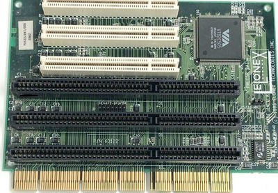
This might fit in here - a riser card for a LPX mainboard with "eisa-like" combined socket and it´s own controller chip VIA VT82C505:
http://www.dosdays.co.uk/media/via/VIA_82C505.pdf

c505.jpg
Filename
c505.jpg
File size
154.69 KiB
Views
190 views
File license
Public domain

The datasheet has a description of the underlying logic.