VOGONS


First post, by oOmDos

User metadata
Rank Newbie
Rank
Newbie

Hi Dear Vogons Community 😀,

I am new to this Forum, and first of all I want to thank you for maintaining this little place, i love reading topics here and today i decided to register myself as well.

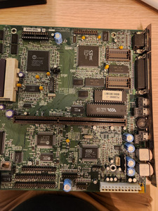
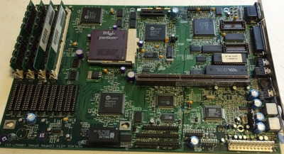
I need your help and knowledge on my case. I baught a Compaq Presario 7170 and Upgraded the CPU from 90 MHZ to 120 MHZ. This was already very tricky because it was not documented how to activate the 120 MHZ CPU.
Luckily I found this post Motherboard won't run P133 at proper mhz where an undocumented PIN Selection will enable it. It works great so far.

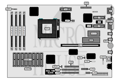
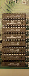
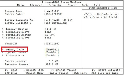
Second I wanted to add L2 Cache so I added 1x Tag and 4 SRAMs. But i have no luck enabling anything on the PhoenixBios 4.04 for the Compaq one. There is no option available in the BIOS. But there are PINS on the Board.
I did try to connect them with a simple cable, but the cache will not be available and can also noch be detected from CACHECHK or CTCM.

The Cache and Tag I Installed is: ISSI - IS61C256AH-20N

What do I need to do in Order to enable the L2 Cache on this Board?

Thank you for your support und helping me with this 😀.

You all have a nice weekend.

Kind regards

Attachments

  • Filename
    33436.pdf
    File size
    322.53 KiB
    Downloads
    30 downloads
    File comment
    Manual
    File license
    CC-BY-4.0
  • Filename
    cache setting.png
    File size
    11.23 KiB
    Downloads
    No downloads
    File comment
    Cache Setting from Manual
    File license
    CC-BY-4.0
  • mb.png
    Filename
    mb.png
    File size
    102.59 KiB
    Views
    934 views
    File comment
    Motherboard
    File license
    CC-BY-4.0
  • 20220910_234459.jpg
    Filename
    20220910_234459.jpg
    File size
    597.22 KiB
    Views
    955 views
    File comment
    Motherboard View Chipsatz
    File license
    CC-BY-4.0
  • 20220917_145104.jpg
    Filename
    20220917_145104.jpg
    File size
    1.37 MiB
    Views
    961 views
    File comment
    Picture of Motherboard where you can see the Caches, Tag and Pin Selection
    File license
    CC-BY-4.0
Last edited by oOmDos on 2022-09-17, 20:11. Edited 1 time in total.

Reply 1 of 36, by majestyk

User metadata
Rank Oldbie
Rank
Oldbie

You have installed 128K L2 cache and a 256 / 32K chip TAG RAM. Normally you don´t install such a large TAG chip here, rather a 128 / 16K or 64 / 8K chip.
Depending on the BIOS it´s possible that the whole cache is disregarded by BIOS because of that.
I´m also sure there´s some jumpering to do to adjust to 128K L2 cache since there a 8 sockets and several possible configurations.

P.S.: According to the silkscreening for JP14 a 128K L2 cache isn´t even supoorted! You need to populate all 8 sockets with 256 / 32K chips for a total of 256K.
Then you can try with 256 TAG, if it doesn´t work reduce TAG size.
Maybe it´s necessary to populate the jumper-pins of JP14 also.

Don´t worry about "TC9".

Reply 2 of 36, by oOmDos

User metadata
Rank Newbie
Rank
Newbie

Hi @majestyk,

Thank you for your repsonse 😀. I did Install 256K of TAG and 1 MB of L2 Cache. And in Pin Select "Table" you can see that i should close PIN 1-2 and 3-4 to set L2 to 1MB. Do I really need to "fill" the complete Bank?

I did Install 4x ISSI - IS61C256AH-20N which are 8x 32k. In the manual it looks Okay. Did I understand something wrong?

I attached new Pictures and a Manual i did find 😀.

Last edited by oOmDos on 2022-09-17, 20:14. Edited 1 time in total.

Reply 3 of 36, by Sphere478

User metadata
Rank l33t++
Rank
l33t++

Are you trying to upgrade to a specific point or to max it out?

Because a k6-3+ 400 mhz could probably be made to work here. And with it you might see better performance with no motherboard cache

Sphere's PCB projects.
-
Sphere’s socket 5/7 cpu collection.
-
SUCCESSFUL K6-2+ to K6-3+ Full Cache Enable Mod
-
Tyan S1564S to S1564D single to dual processor conversion (also s1563 and s1562)

Reply 4 of 36, by majestyk

User metadata
Rank Oldbie
Rank
Oldbie
oOmDos wrote on 2022-09-17, 20:11:

Hi @majestyk,

Thank you for your repsonse 😀. I did Install 256K of TAG and 1 MB of L2 Cache. And in Pin Select "Table" you can see that i should close PIN 1-2 and 3-4 to set L2 to 1MB. Do I really need to "fill" the complete Bank?

I attached new Pictures and a Manual i did find 😀.

The 4 chips you installed don´t make 1MB. You have to divide by 8 to go from bit to Byte. What´s in the silkscreening or manual refers to 256 KByte, 512KByte and 1MByte, while on the chips you have (K)bits.

I´ll give you an example for one chip: One of the ISSI chips has 32768 x 8 bits inside thats 262.144 bits or 256Kbit. Divided by 8 you get 32.768 (32K) Byte per chip.
If you have 4 chips it´s 32KB x 4 = 128KByte in total.

Last edited by majestyk on 2022-09-17, 20:47. Edited 2 times in total.

Reply 5 of 36, by oOmDos

User metadata
Rank Newbie
Rank
Newbie
Sphere478 wrote on 2022-09-17, 20:12:

Are you trying to upgrade to a specific point or to max it out?

Because a k6-3+ 400 mhz could probably be made to work here. And with it you might see better performance with no motherboard cache

I want to add the L2 Kache and stay with the Pentium 120 😀 and also to see the Performance as well.

It is a shame that Compaq did put a Bios with so less functions. It has not even a Menu where I could set Cache settings or anything.

Last edited by oOmDos on 2022-09-17, 20:28. Edited 1 time in total.

Reply 6 of 36, by Sphere478

User metadata
Rank l33t++
Rank
l33t++

Gotcha.

Sounds like majestyk probably has your answer 😀

Sphere's PCB projects.
-
Sphere’s socket 5/7 cpu collection.
-
SUCCESSFUL K6-2+ to K6-3+ Full Cache Enable Mod
-
Tyan S1564S to S1564D single to dual processor conversion (also s1563 and s1562)

Reply 7 of 36, by oOmDos

User metadata
Rank Newbie
Rank
Newbie
majestyk wrote on 2022-09-17, 20:16:
oOmDos wrote on 2022-09-17, 20:11:

Hi @majestyk,

Thank you for your repsonse 😀. I did Install 256K of TAG and 1 MB of L2 Cache. And in Pin Select "Table" you can see that i should close PIN 1-2 and 3-4 to set L2 to 1MB. Do I really need to "fill" the complete Bank?

I attached new Pictures and a Manual i did find 😀.

The 4 chips you installed don´t make 1MB. You have to divide bay 8 to go from bit to Byte. What´s in the silkscreening or manual refers to 256 KByte, 512KByte and 1MByte, while on the chips you have bits.

Ohhh 😁 ! Now I understand. So I need to get "bigger" Chips and also Connect the Pins? Why does the Computer "boot" normaly and not give any errors or "beeps" ?

Reply 8 of 36, by oOmDos

User metadata
Rank Newbie
Rank
Newbie
Sphere478 wrote on 2022-09-17, 20:18:

Gotcha.

Sounds like majestyk probably has your answer 😀

Yes, it seems like. So I get 1 (bigger) Chip for the Tag and also need to add 4 more of the other chips. After that i should have the 256kb. Alternatively complete new chips for it.

Do you have any suggestions which bigger ones to choose ?

Reply 9 of 36, by Sphere478

User metadata
Rank l33t++
Rank
l33t++

You could try the ones I used in my gateway thread

Re: Gateway 2000 overdrive build

But maybe not as that is a 486 class system. I’m sure majestyk will chime in 😀

Sphere's PCB projects.
-
Sphere’s socket 5/7 cpu collection.
-
SUCCESSFUL K6-2+ to K6-3+ Full Cache Enable Mod
-
Tyan S1564S to S1564D single to dual processor conversion (also s1563 and s1562)

Reply 10 of 36, by majestyk

User metadata
Rank Oldbie
Rank
Oldbie

You need 8 of the ISSI chips and a 9th one for TAG to get a total L2-cache size of 256KB. (see example above)
In this case the two jumpers of JP14 stay open so you don´t need to solder there 😀

I don´t think it´s worth upgrading L2 cache to 512KB or even 1024KB. It might be useful if you have a lot of RAM like 128 or 256MB.

One thing is for sure: The new 256KB L2 cache WILL boost the performance.
_____________________________________

Sphere478 wrote on 2022-09-17, 20:24:

You could try the ones I used in my gateway thread

Re: Gateway 2000 overdrive build

But maybe not as that is a 486 class system. I’m sure majestyk will chime in 😀

Those chips are 25nS - might be a bit slow for this pentium setup.
If the clock speed (SB) is 60MHz or 66 MHz I would recommend 15nS cache chips. The current ISSI ones are 20nS - too slow for 66 MHz.

Reply 11 of 36, by oOmDos

User metadata
Rank Newbie
Rank
Newbie

Thank you so much for helping me with this topic @majestyk and also for teaching me all the details. I already love my "old gaming" PC. I spent already two weeks with playing around with it 😁 !

Last edited by oOmDos on 2022-09-17, 21:11. Edited 1 time in total.

Reply 12 of 36, by oOmDos

User metadata
Rank Newbie
Rank
Newbie
majestyk wrote on 2022-09-17, 20:26:
You need 8 of the ISSI chips and a 9th one for TAG to get a total L2-cache size of 256KB. (see example above) In this case the t […]
Show full quote

You need 8 of the ISSI chips and a 9th one for TAG to get a total L2-cache size of 256KB. (see example above)
In this case the two jumpers of JP14 stay open so you don´t need to solder there 😀

I don´t think it´s worth upgrading L2 cache to 512KB or even 1024KB. It might be useful if you have a lot of RAM like 128 or 256MB.

One thing is for sure: The new 256KB L2 cache WILL boost the performance.
_____________________________________

Sphere478 wrote on 2022-09-17, 20:24:

You could try the ones I used in my gateway thread

Re: Gateway 2000 overdrive build

But maybe not as that is a 486 class system. I’m sure majestyk will chime in 😀

Those chips are 25nS - might be a bit slow for this pentium setup.
If the clock speed (SB) is 60MHz or 66 MHz I would recommend 15nS cache chips. The current ISSI ones are 20nS - too slow for 66 MHz.

I found this page and it agrees with your statement that 256k is already plenty of Cache:
https://www.dosdays.co.uk/topics/cache.php

My question is, let say i put 1MB of Cache anyway in it. Will it improve even more ? I could upgrade from 32 to 64MB. Does DOS Support more than 32 MB even? (Currently on 6.22).

Reply 13 of 36, by Sphere478

User metadata
Rank l33t++
Rank
l33t++

Yeah, I was figuring they may be too high ns for pentium class that’s why I mentioned it was 486 class.

Socket 7 boards went all the way down to 4ns on ss7.

I think my s7 mobos are using 6-8ns? I’d have to check.

Sphere's PCB projects.
-
Sphere’s socket 5/7 cpu collection.
-
SUCCESSFUL K6-2+ to K6-3+ Full Cache Enable Mod
-
Tyan S1564S to S1564D single to dual processor conversion (also s1563 and s1562)

Reply 14 of 36, by majestyk

User metadata
Rank Oldbie
Rank
Oldbie

On mainboards with pipleline burst L2 cache the SRAM chips need to be 6 or 7nS for 66 MHz FSB (down to 4nS when FSB is 100 MHz).
Here the maximum FSB is 66 MHz and at the moment - with a 120 MHz Pentium CPU - it´s probably 60 MHz. At the same time L2 cache is not pipeline burst but asynchronous L2 SRAM. So the chips needn´t be that fast, 15nS will be perfect. 20 or 25 are too slow and can cause stability issues depending on the selection (=tolerance) of the chips you pick.

If 512K or 1MB L2 cache have any advantage at a certain amount of RAM at all can only be judged if you have the datasheet / documentation of the UMC chipset that´s being used here.

If you intend to stay with the onboard graphics you should consider doubling video RAM be populating the 2 empty sockets.

Reply 15 of 36, by rasz_pl

User metadata
Rank l33t
Rank
l33t
oOmDos wrote on 2022-09-17, 21:10:

My question is, let say i put 1MB of Cache anyway in it. Will it improve even more ?

diminishing returns. 256 will probably give you 10% speed boost (in anything not write heavy). 512 will add at max 2-3% more, and 1024 in very rare cases up to 1% more.

L1-L2Balance.png
KwPLe.png
Then of course you have to consider kinds of cache, pipelined burst is good 10-20% better than async https://dependency-injection.com/early-pentium-chipsets/

Open Source AT&T Globalyst/NCR/FIC 486-GAC-2 proprietary Cache Module reproduction

Reply 16 of 36, by mkarcher

User metadata
Rank l33t
Rank
l33t

The point of diminishing returns, clearly visible in the post by @rasz_pl depends on the amount of code/data the processor uses repeatedly a lot. This is called the "working set". It seems the working set of the application used to create the miss rate over cache size diagram is just 64KB, but it is not in a contiguous 64KB areas, but sprinkled around the address space. That's why only a fully associative cache is able to cache the full working set at once. You see a big difference between direct-mapped and 2-way associative cache, nevertheless, all typical 386/486/Pentium cache implementations in consumer grade hardware use direct-mapped cache, because the implementation is simpler and thus less expensive.

If you run a game like Duke 3D or Quake, the working set likely depends heavily on texture resolution. If you run a compression tool like 7zip, the working set depends on the dictionary size (which is fixed 32K for ZIP, but variable for the 7z format). A working set of around 64KB seems to be a sensible assumption for 486-era software.

Reply 17 of 36, by oOmDos

User metadata
Rank Newbie
Rank
Newbie

Wow, thank you so much for the great and detailed discussion. I learned so much about it.
So it seems 128 - 256 is aleeady more than enough 😀! It is such a join to read and lesrn about the old Hardware and since i started to play around with the Computer from the 80-90 i start to understand how everythig is evolving in the Computer Industry. I find it very exciting.

Sadly my sram/cache chips arrived and after putting them in i still have no cache available in the system. Nothing in Bios and Cache Checking Software and no inprovement in the Games or Benckmarcks.

I did nix the chips with two different manufacturers and different Timings. Do you think that this is an issue? The oder hast 20ns and the new ones has 15ns.

I really wonder why there are no cache setting in the Bios.

I also found an image in the Internet while doing some research about the PAW-P5600D - I and found some weird wiring. Do you have and Idea what is that wiring for?

Attachments

Reply 18 of 36, by Sphere478

User metadata
Rank l33t++
Rank
l33t++

Bodge wire seems to be something related to ide or sound?

Compare the datasheets of your two chips, see if they have different pinouts.

Tupically different timings alone isn’t enough to be an issue if mobo is set for highest timings

15/20 is pretty high for pentium bus. 🤔

Sphere's PCB projects.
-
Sphere’s socket 5/7 cpu collection.
-
SUCCESSFUL K6-2+ to K6-3+ Full Cache Enable Mod
-
Tyan S1564S to S1564D single to dual processor conversion (also s1563 and s1562)

Reply 19 of 36, by majestyk

User metadata
Rank Oldbie
Rank
Oldbie

You can try setting the frontside bus to 50 MHz temporarily, to "make it easier" for the slower 20nS SRAMS.

Otherwise there might ba a BIOS switch to enable/disable L2 cache that´s hidden and set to "disable" as default. Is there a switch for enabling/disabling L1 cache present?

In Phoenix BIOS 4 rev 6 you would have to expand the menue entry "Memory Cache" (if visible).

phoenix4_6.JPG
Filename
phoenix4_6.JPG
File size
49.05 KiB
Views
685 views
File license
Public domain