VOGONS


Reply 40 of 125, by rasz_pl

User metadata
Rank l33t
Rank
l33t
feipoa wrote on 2022-11-19, 01:18:

Why do you say JP12 pulls down A[31:30]? It is JP13 and JP14 which either pulls A31/A30 up or down. JP12 may be irrelevent to using PB SRAM.

because you said "JP12 is also used to select between 256K and 512K". Bits[7:6] map to A[31:30]
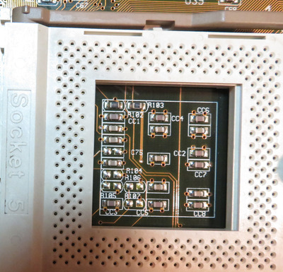
I just saw your Jumper_block.jpg, weird that JP12 goes to tag ram, remove J13-14, keep JP15 if you cut the trace under it

feipoa wrote on 2022-11-19, 03:07:

Just looked at the image of the motherboard I uploaded previously, download/file.php?id=150310&mode=view , I see traces going from TAG to the 74F245 and SRAM in parallel. Should I map them all out, or just put the 74F245 buffers back for another test?

U32 is passing A2-5 A10-11 and probably some other address lines, not what I expected. Now that I think about it I dont know what I expected 😀 but if its address bus then its one way only and they arent needed if not using 5V SRAMs

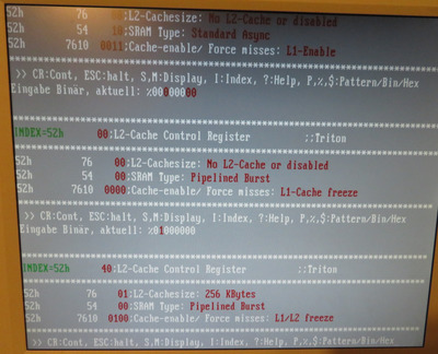
https://usermanual.wiki/Document/intel82430hx … .1819793331.pdf page 4 nice 430HX diagram with PB cache.

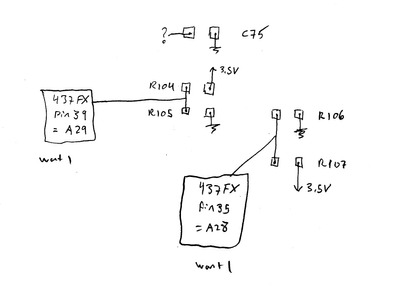
>I traced out chipset pins A29 and A30, but they only go directly to the CPU's A29 and A30. I couldn't find a jumper block where they locate.

Doesnt have to be jumper block if they didnt plan ever using those PB cache footprints, might be just a resistor somewhere and empty resistor footprint somewhere else
Imo its not possible that there is no resistor on those lines if the bios doesnt set this register, something needs to be bootstrapping A29 and A28
A29 is now (SRAM config) pulled to the ground thru a resistor, it needs to be pulled up. Look harder for that resistor 😀
are there any resistors on the back? Measure resistance of pin 39 https://www.digchip.com/datasheets/parts/data … 82437FX-pdf.php to the ground and hmm 3v supply? or CPU Vio?

Last edited by rasz_pl on 2022-11-19, 05:45. Edited 1 time in total.

Open Source AT&T Globalyst/NCR/FIC 486-GAC-2 proprietary Cache Module reproduction

Reply 41 of 125, by feipoa

User metadata
Rank l33t++
Rank
l33t++

Look what I found hidden inside the socket.

Instead of bringing the SRAM type select into a jumper, like Asus did with the SRAM size, they made it hard wired via SMD inside the socket. To set 52H, CC - Cache Control Register [5:4] to [0:0] to Pipeline Burst, we'd pull R104 up to 3.5 V via [presumably] 4.7K and pull R107 up to 3.5 V via 4.7K. Note that I'm pulling them to logic 1 rather than logic 0 because the datasheet says logic levels are inverted,

After a hard reset, CC[7:4] reflect the inverted signal levels on the host address lines A[31 :28].

or am I misinterpret ting this statement?

I'm not sure where the other pad for the vacant C75 goes, but it doesn't go to 5V nor 3.5V. Could it be relevant to getting PBSRAM working?

Asus_under_socket_pinouts.jpg
Filename
Asus_under_socket_pinouts.jpg
File size
97.88 KiB
Views
666 views
File license
CC-BY-4.0
Asus_under_socket_photo.JPG
Filename
Asus_under_socket_photo.JPG
File size
663.01 KiB
Views
666 views
File license
CC-BY-4.0

Plan your life wisely, you'll be dead before you know it.

Reply 42 of 125, by rasz_pl

User metadata
Rank l33t
Rank
l33t

hmm, with R105 missing now how would cache get initialized if bios doesnt set that register either?
measure A29 resistance to ground, if its not <10Kohm just solder R104 and we should be good

Open Source AT&T Globalyst/NCR/FIC 486-GAC-2 proprietary Cache Module reproduction

Reply 43 of 125, by feipoa

User metadata
Rank l33t++
Rank
l33t++

Yeah, I was also wondering how the chipset gets set into Async mode. As noted, 52h is missing from the BIOS. Perhaps some versions of the chipset have 52h defaulting to 00100010 rather than what is stated in the manual, which is SSSS0010. Or floating bits for [7:4] get defaulted to 0010. I don't know.

I measured 437FX pin 39 (which is A29) resistance to GND, 3.5V, 5.0V and they all were 40 M-ohms. I also measured 437FX pin 35 (which is A28) to GND, 3.5V, 5.0V and they all were 34 M-ohm.

Next I will try soldering 4.7K onto R104. Boot. If fail, also solder 4.7K onto R107. If fail, set JP13 to 0 and JP14 to 1. If still fails, try my modded BIOS for 52h. Maybe try soldering the 245 chips back? Look for more hardcoded changes for PBSRAM settings?

Plan your life wisely, you'll be dead before you know it.

Reply 44 of 125, by feipoa

User metadata
Rank l33t++
Rank
l33t++

The socket area on the only photo we have of this board with PBSRAM looks to have R104, R105, R106, and R107 empty. This is troubling me. SMD 0805 pads that are populated don't have the skinny black strip showing up on the photos. If there's not another vacant SMD pad which sets [A29:A28], there may very well have been a PBSRAM specific BIOS for this board.

Asus_PB_board_socket_area.png
Filename
Asus_PB_board_socket_area.png
File size
170.13 KiB
Views
638 views
File license
CC-BY-4.0

Plan your life wisely, you'll be dead before you know it.

Reply 45 of 125, by majestyk

User metadata
Rank Oldbie
Rank
Oldbie

In case you haven´t tried yet, here are two older BIOS versions for this board:

Filename
tx5i0202.zip
File size
83.27 KiB
Downloads
26 downloads
File license
Public domain
Filename
tx5i0115.zip
File size
75.95 KiB
Downloads
24 downloads
File license
Public domain

In the manual they note that the board is equipped with either async or pb RAM and that you cannot use both at the same time. There´s no mention of different BIOSes.

I just flipped through the pictures of my own mainboards and found several FX boards that can be populated either with DIL chips or a COAST module (which means PB-SRAM plus TAG) and on all of them the two Transceiver chips are present regardless of what´s running (TAG gets removed when the COAST brings it´s own TAG). So the two chips at least don´t hurt. Question is if they are needed for PB-SRAM mode.
They are soldered in no time - give it a try...

Reply 46 of 125, by feipoa

User metadata
Rank l33t++
Rank
l33t++

I've tried all BIOSes I could find, which are:

MR BIOS
103
106
115
202
302.008 beta
302
302+IDE 128GB

Each show no cache installed at POST. I also checked their chipset register settings and they all are missing 52h.

I installed 4.7K at R104 and R107 to set L2 type to pipeline burst:

R104_and_R107_populated.JPG
Filename
R104_and_R107_populated.JPG
File size
250.18 KiB
Views
612 views
File license
CC-BY-4.0

I also set JP13 to GND via 4.7K @ R57 and JP14 to VCC via 4.7K @ R60 to set size register to 256K L2.

None of this altered the state of register 52h when checking with CTCHIP34. I tried my hacked BIOS to force 256K and pipeline burst, but screen stayed blank. Same as before.

I re-soldered the 245 chips - didn't help.

Should the pull-downs to GND be shorts rather than 4.7K ?

I tried setting L2 to Burst SRAM rather than Pipeline Burst SRAM, but didn't help.

Maybe the UMC PBSRAM has some incompatibility with this MB?

I can have CTCHIP34 set the 256K register bit and the pipeline register bit fine, but the issue comes when I try to adjust SCFMI and FLCE (bits 1 & 0 of 52h) from their default value of 11 to 10. This essentially enables L2. And hangs the system.

I should point out that after I set SRAM to PBSRAM and L2 to 256K, CTCHIP34 complains about the SCFMI and FLCE values, it says:

L1 enabled, L2 force miss on read/write (incoherent!)

I suspect there's some components on the motherboard, like shorts, resistors, etc., which need to be altered for the case of using PBSRAM. Unfortunately, I have no reference to find these alterations. Defeat is feeling eminent. Any other ideas?

Plan your life wisely, you'll be dead before you know it.

Reply 47 of 125, by majestyk

User metadata
Rank Oldbie
Rank
Oldbie

In the 430HX documentation there is a table for SCFMI and FLCI that has the values the other way round than you need to enter them in the 52h string. (See the last post in my 512MB HX story).
Maybe that´s also true in your FX documentation?

Reply 48 of 125, by feipoa

User metadata
Rank l33t++
Rank
l33t++

In looking through the manuals of 430FX boards which have a COAST slot and DIP sockets for SRAM, there is a repeating theme - one jumper to select between the DIP SRAM and the COAST slot. Maybe there is something like the the feature on the Am386DX which lets you disable all pins. ON the Am386DX, I think setting FLT# to GND disables the whole chip by floating all the pins. Perhaps there is a similar occurrence with QFP-100 SBSRAM?

According to the datasheet for my UMC UM61L3232 PBSRAM modules, the most relevant sounding pins are:

Chip Enable CE2#, CE2, CE#

CE# is active low, and I presume CE2# is active low? CE2 presumably is active high. Why are there 3 chip enable pins? Should these be static throughout power-on, that is, all of them active?

Asynchronous Power Down (Snooze): High = sleep, Low or NC = Wake up.

I also noticed that for boards with both COAST and DIP SRAM slots/sockets, the 245 chips remain in place. However, boards pre-configured with a COAST slot and unpopulated DIP pads tend not to have the 245 chips.

Attachments

Plan your life wisely, you'll be dead before you know it.

Reply 49 of 125, by feipoa

User metadata
Rank l33t++
Rank
l33t++
majestyk wrote on 2022-11-19, 14:52:

In the 430HX documentation there is a table for SCFMI and FLCI that has the values the other way round than you need to enter them in the 52h string. (See the last post in my 512MB HX story).
Maybe that´s also true in your FX documentation?

majestyk, the 430FX manual states the signals on the host address lines A[31:28] be inverted. So for the table you presented, e.g. for 256K PBSRAM with A31:A30:A29:A28 = 1:0:1:1, and if invert these to 0:1:0:0, this cooresponds to the 52h register bit values for 256K PBSRAM.

If you take the values not inverted, looking again at page 22 of the 430FX manual, then 1:0:1:1 cooresponds to 512K, dual-bank pipelineburst 512K SRAM.

Note that I also tried the jumpers flipped, as the resistors under the CPU, just in case. It didn't help the situation.

EDIT: Regarding SCFMI and FLCE, look at the table on page 23. Also note that the table is presented in the wrong order, it is putting FLCE before SCFMI, so to put them back into the register bit order, you need to flip those two columns. I think this is why you think values are reversed.

The ideal setting for 52h should be 0100XX01. But bear in mind that I have tried all combinations for FLCE and SCFMI.

Attachments

Plan your life wisely, you'll be dead before you know it.

Reply 50 of 125, by rasz_pl

User metadata
Rank l33t
Rank
l33t
feipoa wrote on 2022-11-19, 13:41:

None of this altered the state of register 52h when checking with CTCHIP34.

entirely possible its hardcoded in cache enabling procedure of the POST
C6 Cache Presence Test; External cache size detection
09 Early Cache Initialisation. Cyrix CPU Initialisation. Cache Initialisation

Its possible no jumpers/resistors are needed because bios tries to auto detect cache type and size. Would be great to compare with
https://theretroweb.com/motherboards/s/asus-p … xe-ver.-2.4-2.5

feipoa wrote on 2022-11-19, 13:41:

I tried my hacked BIOS to force 256K and pipeline burst, but screen stayed blank. Same as before.

its understandable without knowing when bios applies those registers - Im now 99% sure you need special cache flush/disable/enable procedure to change it on a live system, there are rules about 52h bits when enabling it 430FX_52h.png

> I see the settings for 52h are: 0010XX11

I would try changing it bit by bit by setting it to 00000000, 01000000, 01000001
or other way around, 00000000, 00000001, 01000001

feipoa wrote on 2022-11-19, 13:41:

I re-soldered the 245 chips - didn't help.

buzzing where its going would help in understanding buffer purpose, the couple of traces I could follow on the picture suggest address bus, so its possible its there only to convert 3.3V address bus up to 5V for the 5V SRAM async cache chips. Does 245 supply voltage go thru those "mixed voltage/sram voltage" jumpers?

feipoa wrote on 2022-11-19, 13:41:

Should the pull-downs to GND be shorts rather than 4.7K ?

its address bus, those are bootstraps, if you pull down hard nothing will be ale to change those address lines and chipset/cpu output buffers might burn down while trying to fight with hard pulldown.
Besides we dont need a pull down, we need a pull up R104

feipoa wrote on 2022-11-19, 13:41:

I can have CTCHIP34 set the 256K register bit and the pipeline register bit fine, but the issue comes when I try to adjust SCFMI and FLCE (bits 1 & 0 of 52h) from their default value of 11 to 10. This essentially enables L2. And hangs the system.

why is it 11 in the first place. 11 is "Enabled; miss forced on reads/writes", try 00 first

feipoa wrote on 2022-11-19, 13:41:
I should point out that after I set SRAM to PBSRAM and L2 to 256K, CTCHIP34 complains about the SCFMI and FLCE values, it says: […]
Show full quote

I should point out that after I set SRAM to PBSRAM and L2 to 256K, CTCHIP34 complains about the SCFMI and FLCE values, it says:

L1 enabled, L2 force miss on read/write (incoherent!)

yes, because 11 is bad

Open Source AT&T Globalyst/NCR/FIC 486-GAC-2 proprietary Cache Module reproduction

Reply 51 of 125, by feipoa

User metadata
Rank l33t++
Rank
l33t++

The manual for the 6 month newer version of this board, P/I-P55TP4XE*, indicates that JP12 is indeed only for Asynchronous setting. This was already discovered by tracing the pins earlier. What it does have, is JP16 with 1-2 = enable, and 2-3 = disable. The manual states,

if the L2 cache is Asynchronous SRAM installed in the sockets on the mainboard, you must enable the onboard sockets with this jumper. If the L2 cache is a cache module (COAST), disable this jumper.  This jumper is for Revision 2.4 Only.

I'd like to know where JP16 goes. Curious that the earlier revisions of the PCB, don't have JP16 at all, only JP12.

I was also wondering how 52h gets 11 set for SCFMI/FLCE.

I tried the BIOS for P/I-P55TP4XEG v302, but screen stays blank with the same POST code as when I use my hacked PCI/I-P54TP4 BIOS. Curiously, the BIOS for P/I-P55TP4XE v302 works, but still no L2 cache detected and CTCHIP34 hangs when enabling.

If I try the order for 52h, 0000XX00, then 0100XX00, no complaints

IMG_0770.JPG
Filename
IMG_0770.JPG
File size
364.72 KiB
Views
556 views
File license
CC-BY-4.0

and when running cachechk, L1/L2 disabled as expected,

IMG_0771.JPG
Filename
IMG_0771.JPG
File size
405.48 KiB
Views
556 views
File license
CC-BY-4.0

but when I then add 0100XX01, the system hangs with

Unknown Opcode Error aufgetreten, ctch h   h   h   h
IMG_0773.JPG
Filename
IMG_0773.JPG
File size
122.57 KiB
Views
556 views
File license
CC-BY-4.0

Regarding those SRAM jumpers:
MIX SRAM - this just sets 5V to the Asynchronous SRAM DIPs, VCC - but not the TAG
3.3V SRAM - this just sets 3.5V (or whatever voltage the VRM is set to) to the Asynchronous SRAM DIPs, VCC - but not the TAG

Regarding the 74F245 buffers:
SRAM address pins funnel thru the 245 chips, not I/O pins. I didn't measure the others.
SRAM TAG address pins fulley through the 245 chips, no I/O pins. I didn't measure the others.

Yes, most are pull-ups, but there is one pull-down needed - JP13 we want logic 0 for A30, so pull-down through R57. Inverting logic 0 is logic 1, and this corresponds to 52h bit 6.

Edit:
I traced out chip enable pins on UM61L3232 PBSRAM chip.
CE2# is hard coded to GND
CE2 is hard coded to 3.5V
CE# is controlled by pin24 of the 430FX chipset. Pin24 is listed as CCS#/CAB4

The Asynchronous Power Down (snooze) pin on the UM61L3232 is left N/C, which appears to leave the chip in the AWAKE state.

Plan your life wisely, you'll be dead before you know it.

Reply 52 of 125, by rasz_pl

User metadata
Rank l33t
Rank
l33t
feipoa wrote on 2022-11-20, 04:06:
but when I then add 0100XX01, the system hangs with […]
Show full quote

but when I then add 0100XX01, the system hangs with

Unknown Opcode Error aufgetreten, ctch h   h   h   h

looks like enabling cache is working? but your cache chips contain random data, some kind of cache initialization/flush procedure while 0100XX11 needed first to bring flash in line with ram contents?

feipoa wrote on 2022-11-20, 04:06:

Regarding those SRAM jumpers:
MIX SRAM - this just sets 5V to the Asynchronous SRAM DIPs, VCC - but not the TAG
3.3V SRAM - this just sets 3.5V (or whatever voltage the VRM is set to) to the Asynchronous SRAM DIPs, VCC - but not the TAG

arent 245 buffers also powered by the same trace as Async sram?

Have you dried MR BIOS with R104 soldered?
I still suck at disassembling bioses with sourcer, would need Chkcpu help to see what exactly is bios doing.

Open Source AT&T Globalyst/NCR/FIC 486-GAC-2 proprietary Cache Module reproduction

Reply 53 of 125, by feipoa

User metadata
Rank l33t++
Rank
l33t++

VCC on the 245 buffers is tied directly to 5V, not the MIX SRAM or 3.3V SRAM jumpers. From what I can detemrine, it is only the DIP SRAM sockets, but not the TAG, which is going to those jumpers

I suspect the cache is functioning, but there's one more point on the board that is corrupting the data which needs to be address. I suspect this point is a hardware related - a trace, or component needing to be removed/added.

I currently have R57 and R59 populated via JP14/JP13, meaning A31:A30 = [1:0], inverted = 54h bits [7:6] = [0:1] = 256K SRAM. CTCHIP34 shows [0:0]

I currently have R104 and R107 populated inside the socket, meaning A29:A28 = [1:1], inverted = 54h bits [5:4] = [0:0] = Pipelined Burst. CTCHIP34 shows [1:0]

I currently have JP15 installed, meaning 52h bit [3] has NA# set high, or logic [1]. CTCHIP34 shows [0].

It is very curious how all of these settings are being ignored and seemingly overwritten. You are probably right that it is an auto-detect BIOS routine, but that routine is probably determining that the cache isn't functioning properly. I'll try the MR BIOS one more time with the above hardware settings.

I'd really like to know what the jumper on these dual ASYNC/PBSRAM 430FX boards is setting to enable/disable the ASYNC SRAM. I have sent that vswitchzero youtube guy a message via his website's contact form a few days ago, but no reply.

Plan your life wisely, you'll be dead before you know it.

Reply 54 of 125, by rasz_pl

User metadata
Rank l33t
Rank
l33t

I could probably write few byte long test file that when flashed as bios would display on POST card default contents of 52h, no idea if there is any point to it tho if bios autodetect overrides it anyway

Open Source AT&T Globalyst/NCR/FIC 486-GAC-2 proprietary Cache Module reproduction

Reply 55 of 125, by majestyk

User metadata
Rank Oldbie
Rank
Oldbie

I think the picture of the PB-Burst version I found comes from this Japanese website:
https://lavista.hatenablog.com/entry/2021/10/21/141043
It also came with a 3.5" floppy labeled "BIOS Upgrade Diskette 1.2". (Maybe there existed 2 versions of 1.2 BIOS?)

If you throw the text into a translator you can read the guy who owns it worked for some pr-agency or magazine back then and the Asus PCI/I-P54TP4 was the first ever PB-Burst cache mainboard to be released. He also says there were only 200 copies produced.
Reading that I wouldn´t be surprised if there was a special BIOS for this version that´s unknown today.
And we wouldn´t know if that BIOS had some routine (probing) for PB at all or if it was PB-Burst only.
I would suggest to test all kinds of BIOSes for FX mainboards that were PB-only.

Reply 56 of 125, by feipoa

User metadata
Rank l33t++
Rank
l33t++

With R104, R107, JP13, and JP14 set, the MR BIOS setup still shows no external L2 cache. However, when looking at the options set for CTCHIP34, MR BIOS has Pipelined Burst mode set correctly, and SCFMI/FLCE. However, it has the L2 cache size (52h bits 7:6) set to "no cache". When telling CTCHIP34 that the L2 cache size is 256K, the system hangs up.

I am guessing that Asus and MR BIOS try to enable the cache, but an error is reported, and they disable the cache. It is just that Asus is disabling the L2 using different 52h register bits compared to MR BIOS.

CTCHIP34 reports 52h for bits [7:6:5:4:3:2:1:0] as,

ASUS: 0010xx11
MRBIOS: 0000xx01
desired: 0100xx01

The result above is for the Asus PCI/I-P54TP4 v302 BIOS, but the P/I-P55TP4XE v302 BIOS had the same, that is, 0010xx11.

majestyk, nice detective work. The Asus board which came after the PCI/I-P54TP4 was the P/I-P55TP4XE. The P/I-P55TP4XE has Async DIP sockets and a COAST socket. The jumper JP16 is used to "enable/disable the DIP sockets". I'd like to know where that jumper goes. When I pulled up the PCI/I-P54TP4 v302 BIOS and the P/I-P55TP4XE V302 BIOS, their checksum, as shown in Awdbedit is the same as is the BIOS string. Thus, the BIOS I have been testing should work with PB cache. It is possible that this "first ever PB-Burst cache mainboard to be released" requires some obscure PB cache modules with perhaps a pin or two difference from what was mainstream 6-12 mo. later.

Plan your life wisely, you'll be dead before you know it.

Reply 58 of 125, by TheMobRules

User metadata
Rank Oldbie
Rank
Oldbie
feipoa wrote on 2022-11-21, 07:00:

The Asus board which came after the PCI/I-P54TP4 was the P/I-P55TP4XE. The P/I-P55TP4XE has Async DIP sockets and a COAST socket. The jumper JP16 is used to "enable/disable the DIP sockets". I'd like to know where that jumper goes.

I have a P/I-P55TP4XE with a 256KB PB cache module (judging from the dates on the chips and PCB, it appears to be from early to mid 1995). Is there anything you'd be interested in comparing vs. your board?

Reply 59 of 125, by rasz_pl

User metadata
Rank l33t
Rank
l33t

btw Im getting close while struggling in ida, finally found:

_F000:E4E7                 mov     al, 0C1h ; '-'
_F000:E4E9 mov dx, 80h ; 'Ç'
_F000:E4EC out dx, al ; manufacture's diagnostic checkpoint

Late Award BIOS (4-5x PnP)
C1 Auto detection of onboard DRAM & Cache

TheMobRules wrote on 2022-11-21, 07:25:

I have a P/I-P55TP4XE with a 256KB PB cache module (judging from the dates on the chips and PCB, it appears to be from early to mid 1995). Is there anything you'd be interested in comparing vs. your board?

downloading CTCHIP34, reading value of register 52h, trying to change that value to all 00000000, exiting CTCHIP34, trying to play a short round of some big game or starting windows, exiting game/windows, running CTCHIP34 again and trying to set register 52h to the same value you had at the start. I want to know if computer will freeze or happily run 😀

Last edited by rasz_pl on 2022-11-21, 08:18. Edited 2 times in total.

Open Source AT&T Globalyst/NCR/FIC 486-GAC-2 proprietary Cache Module reproduction