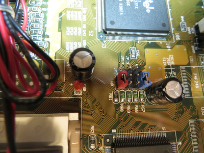
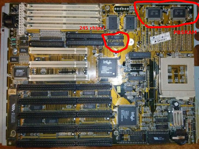
majestyk, I'm starting to wonder if that photo you found of the P54TP4 w/PB SRAM is correct. Is that a stock image from Asus? Where did you find it? When I look at the traces, I see traces going between the TAG chip and the 74F245 chip, as well as traces going from the 74F245 chip to the PB SRAM chip. Should I solder them back on?
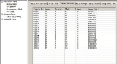
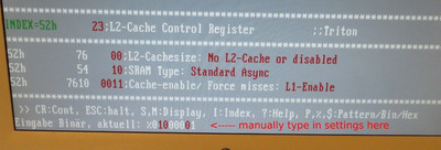
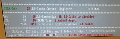
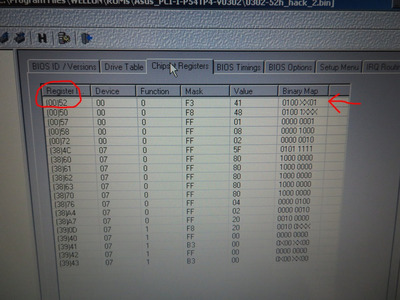
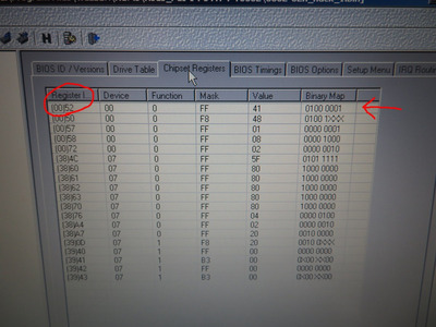
After I ran CTCHIP34, I see the settings for 52h are: 0010XX11. I think they are supposed to be: 0100XX01. When I force this setting, CTCHIP hangs.
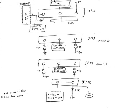
I cut the NA#, or JP15 trace, however screen stays blank with it cut. I then soldered on the remaining jumpers, JP13-JP15, as well as four 0805 SMD 4.7 K-ohm resistors. Two are pull-up to 3.5 V, while the other two are pull-down to GND.
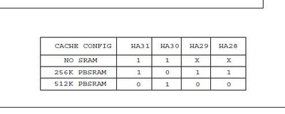
I set the jumpers on JP13: 1-2, JP14: 1-2, which should equate to 256K SRAM, but CTCHIP still shows L2 disabled. I tried JP13 and JP14 on 2-3, but CTCHIP still showed L2 disabled.
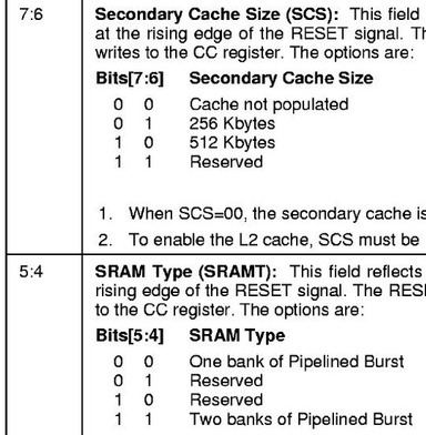
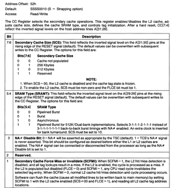
The pinouts for the jumper block is shown below. Unfortunately, there is nothing that goes to A29 or A28, which would set the SRAM type to Pipeline Burst. CTCHIP34 shows the SRAM type as Async.
I traced out chipset pins A29 and A30, but they only go directly to the CPU's A29 and A30. I couldn't find a jumper block where they locate.
Plan your life wisely, you'll be dead before you know it.