VOGONS


First post, by foil_fresh

User metadata
Rank Member
Rank
Member

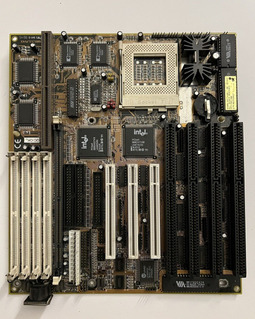
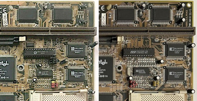
Just bought this motherboard without properly checking to see if there is doco out there and if also to confirm the cache is real.

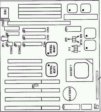
It looks like it should be called the 5i-VX1 as per https://theretroweb.com/motherboards/s/lucky-star-5i-vx1 but the board clearly says LS_P54CE next to Model on the silkscreen. Does anyone have one and can confirm?

I'm after the pinout for the PS/2 port and any other jumper settings related. There is a doco in Russian in the same link but I cant be sure; JP3 might be an on/off for PS/2 mouse?

I have a spare COAST from an IBM PC350 that uses a similar intel chipset. Are these COAST modules usually interchangable when it comes to intel?

Any info is helpful. Cheers.

Attachments

Reply 1 of 5, by snufkin

User metadata
Rank Oldbie
Rank
Oldbie

I think it's more likely to be the P54CE: https://theretroweb.com/motherboards/s/lucky- … rev-f#downloads

COAST modules are not guaranteed to be interchangeable, so you may need to check where Ground and Power are. There was a thread here with a couple of pinouts: Pentium COAST / CELP L2 cache sticks standards

Reply 2 of 5, by foil_fresh

User metadata
Rank Member
Rank
Member

Thanks snufkin.

I believe I'm on top of the Ps2 port pinout - I checked virtually every socket 7 lucky star motherboard doco i could find and they all have the same pinout. Gonna trust that its the same again for this.

Reply 3 of 5, by majestyk

User metadata
Rank Oldbie
Rank
Oldbie

Where´s the "fake cache" supposed to be?

I see two Galvantech SRAMS -> real cache.
two Intel transceivers/ buffers -> have nothing to do with cache
and a COAST slot -2nd half of 512K real cache except when you would insert a fake COAST module. I have never seen such a module.

Reply 4 of 5, by foil_fresh

User metadata
Rank Member
Rank
Member

the 3rd image attached - there's no markings on the top chips above the COAST slot. just black plastic. thats what i was concerned about. if those are not related to cache then I am happy that its not an issue 😀 thanks

Reply 5 of 5, by snufkin

User metadata
Rank Oldbie
Rank
Oldbie
foil_fresh wrote on 2022-12-10, 13:52:

I believe I'm on top of the Ps2 port pinout - I checked virtually every socket 7 lucky star motherboard doco i could find and they all have the same pinout. Gonna trust that its the same again for this.

You should be able to ID which pins are +5 and GND with the board off by measuring resistance to ground and +5 on either the keyboard or power connector. That just leaves clock and data, so worst case is just try one and if it doesn't work swap them round. That said, it's likely they'll have reused the same pinout.

[edit to add: I think those two chips are part of the Intel chipset, 82438VX. Can see the faint Intel 'i']

[curious, comparing the photo of your board with one of the ones on RetroWeb, and they're bother marked P54CE, but the jumpers between the CPU and cache are different. In particular, yours doesn't seem to have any jumpers for setting the cache size.

Also, I've had a go at a translation (or rather, Google had a go) of that Russian sheet on the VX1:

Filename
LS_VX1.pdf
File size
101.44 KiB
Downloads
37 downloads
File license
Fair use/fair dealing exception

But, no information about JP1, CN2 (I assume the PS/2 header) or JP15 (clear CMOS maybe?)

[last edit... Looks like yours has more options for bus speed compared the other one

P54CE.jpg
Filename
P54CE.jpg
File size
216.68 KiB
Views
365 views
File license
Fair use/fair dealing exception