VOGONS


First post, by mbarszcz

User metadata
Rank Newbie
Rank
Newbie

I have an M912 v1.7 motherboard that originally came with fake cache. This board was in rough shape when I got it, the system would barely make it past POST. Turns out that in addition to the fake cache, it had a bad voltage regulator and some questionable caps which were causing the instability. After fixing that up, and replacing the fake cache with sockets, pin headers, 512K of real cache, and a BIOS upgrade, it has really come a long way. Now it is solid as a rock and runs so much better than it did before. With L2 cache, it is so much more usable.

The board came with an Am486 DX2-80 installed, and as I mentioned, I was able to upgrade the bios to the 1995X bios. All that went surprisingly without issue.

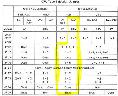
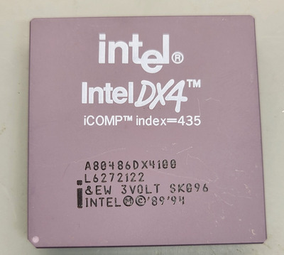
I decided to take it up another notch and upgrade the DX2-80 to an Intel DX4-100 (SK096). I set the jumpers as per the table in the manual for an Intel DX4 (see screenshot), plus the jumpers for VL Bus no wait states and to 33MHz.

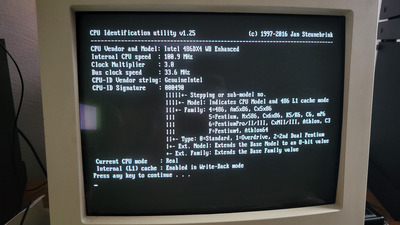
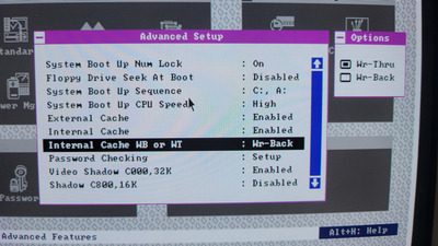
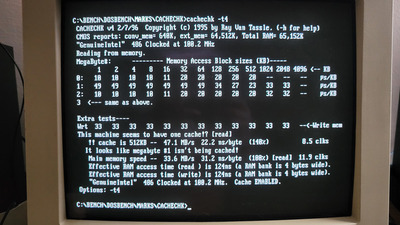
The system came up, and I set timings set to 2-1-1-1 with no ram or cache wait states, and everything seemed to be working solid in write-thru mode. When I enabled L1 write-back in the bios options, things started to get goofy. cachechk reported that the first 1MB wasn't cached, cachechk in write mode showed steady performance across the block sizes (indicating effectively write-thru mode), chkcpu still showed write-through mode, and the quake and chris's 3d benchmark ran very poorly. After resetting it back to write-thru mode, everything seems back to normal.

So with that in mind, it seems that the CPU/board run fine in write-thru, but for some reason, write-back isn't properly supported and starts causing strange behavior.

Since the CPU was a China ebay special, I took the CPU out and gave it a good scrub with some acetone to make sure it wasn't relabeled, and it certainly looks legit, no signs of re-markings. The label is engraved in the CPU, not just screen printed on. This thread seemed similar to my situation, but in the end it turns out the guy had a fake CPU PC Chips M912 BIOS update for Am5x86 and Cyrix 5x86

With the chip saying &EW on it and cpu-world.com saying that the chip supports write-back https://www.cpu-world.com/sspec/SK/SK096.html, it certainly seems that this setup should be capable of write-back mode.

Other things I've tried with no success:
- Fiddling with the undocumented jumper JP36 (that just causes the L2 cache to be detected as 32K but not work)
- Using the Award BIOS instead of the AMI BIOS
- Modifying the Award Bios to force write-back mode (this didn't work and still came up as a grayed out as the grayed out write-thru option. It's like the board doesn't know what to do when write-back mode is forced on it.

Does anyone have an M912 1.7 working in write-back mode successfully, even better with a DX4-100? Any ideas what I might be missing?

Attachments

Reply 1 of 7, by Chkcpu

User metadata
Rank Member
Rank
Member

Hi mbarszcz,

I believe you missed a few jumper settings. 😉
The L1 cache WB mode of Intel and AMD 486 CPUs is controlled by jumpers and not by the BIOS.
The L1 cache WT/WB option in the BIOS is controlling the chipset and for software control of WB mode on Cyrix CPUs.

For an Intel 486DX4 WB, you have to use the P24D jumpers for CPU Type Selection:

JP27: 1-2, 3-4
JP28: 1-2, 4-5
JP29: 1-2, 4-5
JP30: 3-4, 5-6
JP32: 1-2
JP33: 1-2, 3-4

The other jumper settings should remain the same as for a DX4-100, so 3.3V Vcore, 33MHz FSB and x3 multiplier.
With the above settings, and a CPU that supports WB, the CPU should operate in L1 cache WB mode and my CHKCPU tool should clearly tell you so. 😀

Then of course you need to run a BIOS that support this, like the AMI 1995X or the patched Award M912_J2 BIOS from Re: PC Chips M912 BIOS update for Am5x86 and Cyrix 5x86

Please let us know if this works.
Jan

CPU Identification utility
The Unofficial K6-2+ / K6-III+ page

Reply 2 of 7, by mbarszcz

User metadata
Rank Newbie
Rank
Newbie

Hi Jan, Thanks for making the CHKCPU utility 😀 I am running the AMI 1995X BIOS (the board came with the original 1994 bios ROM.

I would have never in a million years guessed that those would have been the right jumper settings to pick, but you were right. After setting them, ckhcpu now shows the correct CPU and WB mode just like you said. How is it that chkcpu actually shows a different CPU-ID when the jumpers are in the wrong position? I would have thought that it would have read that off the chip just the same. With the jumpers in the wrong position, I believe it showed as 0483 before (or 0480, can't quite remember, but it definitely wasn't 0490 before).

CHKCPU.jpg
Filename
CHKCPU.jpg
File size
1.61 MiB
Views
384 views
File comment
CHKCPU after setting the jumpers
File license
CC-BY-4.0

Unforunately even with it showing up correctly in write-back mode there is still the same same strange behavior though when the bios is set to write-back mode.

tmp-1671901429508_copy.jpg
Filename
tmp-1671901429508_copy.jpg
File size
1.07 MiB
Views
384 views
File comment
Bios Settings
File license
CC-BY-4.0

You mentioned that the jumpers control the CPU and the BIOS controls the chipset/software control. Somehow the chipset setting seems to still be messing things up. Even with the jumpers in the correct position, having write-back enabled in the bios causes Chris's 3D benchmark to run really slow (7.6fps instead of 48fps), and cachechk to report the following error "It looks like megabyte #1 isn't being cached".

cachechk.jpg
Filename
cachechk.jpg
File size
609.84 KiB
Views
384 views
File license
CC-BY-4.0

Speedsys also shows steady slow write throughput performance with no cache "steps" in the graph.

Setting the bios to write-thru causes the system to work normally again (and ckhcpu still reports it being in write-back mode), but it still doesn't appear to actually be using write-back mode, unless I just don't know what I'm looking for 🤔 (wihch is also a very real possibility).

Reply 3 of 7, by Chkcpu

User metadata
Rank Member
Rank
Member

Okay, you got the CPU in L1 cache WB mode, great! 😀

Yes, it is true that Write-Back capable Intel and AMD 486 CPUs will change their CPUID Signature depending on the L1 cache mode. CHKCPU knows these CPUID values and translates them in readable English for the L1 cache mode display.
Note that Cyrix 486/5x86 CPUs don’t support CPUID, but these CPUs have another mechanism to report the WB mode so CHKCPU can display this info on Cyrix CPUs as well.

This AMI BIOS behavior on Internal cache Wr-Back option is strange indeed.
Can other M912 users chime in here to confirm this BIOS behavior?

I’m unfamiliar with the inner workings of the AMI WinBIOS, but on the Award BIOS for the UMC498 chipset I know that this option is functional on Cyrix CPUs only and is used to program the Cyrix CPU for WB mode.

I know from other 486 chipsets that the BIOS also needs to control specific chipset registers to enable L1 cache WB mode, but I never found this logic in BIOSes for UMC498. I assume the UMC498 doesn’t need this programming and is always “on” to receive signals from a WB capable CPU, but because datasheets for UMC498 are nowhere to be found, this is just a guess.

When using the AMI BIOS, just keep the Internal cache option on Wr-through for now.
You can test the correct functioning of the L1 cache WB mode by booting from a DOS 6.x floppy. If you don’t get a hang here, the chipset/CPU interface for L1 cache WB mode works correctly.

Merry Christmas,
Jan

CPU Identification utility
The Unofficial K6-2+ / K6-III+ page

Reply 4 of 7, by Sphere478

User metadata
Rank l33t++
Rank
l33t++

Weren’t there wb and non wb versions of the dx4? How do you tell from the markings?

Sphere's PCB projects.
-
Sphere’s socket 5/7 cpu collection.
-
SUCCESSFUL K6-2+ to K6-3+ Full Cache Enable Mod
-
Tyan S1564S to S1564D single to dual processor conversion (also s1563 and s1562)

Reply 5 of 7, by mbarszcz

User metadata
Rank Newbie
Rank
Newbie
Sphere478 wrote on 2022-12-25, 01:39:

Weren’t there wb and non wb versions of the dx4? How do you tell from the markings?

The &EW on the chip is supposed to indicate writeback, &E means write through.

Reply 6 of 7, by Sphere478

User metadata
Rank l33t++
Rank
l33t++

Gotcha. Thx

Sphere's PCB projects.
-
Sphere’s socket 5/7 cpu collection.
-
SUCCESSFUL K6-2+ to K6-3+ Full Cache Enable Mod
-
Tyan S1564S to S1564D single to dual processor conversion (also s1563 and s1562)

Reply 7 of 7, by Disruptor

User metadata
Rank Oldbie
Rank
Oldbie

On AMD it's the difference between V8T, NV8T (WT) and SV8B (WB).
Note that the WT 486 from AMD needs to be jumpered like a DX2 (with 3.3 Volt!) and the WB 486 like the Intel DX4 (3.3 Volt too!).