Reply 80 of 108, by mkarcher
feipoa wrote on 2023-06-18, 09:03:Very interesting discovery about cache contents being kept valid while it is disabled.
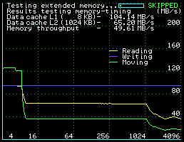
I will try EDO 3-1-1-1 at FSB60 and 0ws/0ws with L2 removed. Since the margin for Cyrix != margin for AMD, I think this test is worth a shot. Or have you already tried this at 2x60 w/Am5x86?
I'm gonna call the mode that keeps the cache valid "standby" instead of disabled, to differentiate between them. With the Cyrix, I was barely able to get 3-1-1-1 working in the winter with L2 removed at 3*40 MHz, in the summer, I'm was able to get 3-1-1-1 with cache removed using an AMD DX4 120 at 4*30, but not at 2*60.
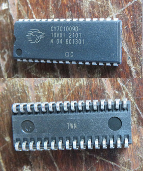
feipoa wrote on 2023-06-18, 09:03:mkarcher wrote on 2023-06-17, 11:10:I have a good old HiLo ALL-03A EPROM/GAL/Flash programmer. It might be a good idea to add a SOJ-to-DIP adapter to it, to be able to test the SRAM chips.
Do you know where to buy one? I have a two different programmers with 20 or so adaptors, but neither had a SOJ 300mil to DIP adaptor.
No idea, I'm sorry. I didn't yet search for one.
feipoa wrote on 2023-06-18, 09:03:mkarcher wrote on 2023-06-17, 17:20:But there is a distinct "cache disabled" mode that does not touch the data SRAM, which is different from the "cache in standby" mode I presumed to be the "most disabled" mode that is available.
When I set L2 to disabled in the BIOS (and still have L2 installed), is the L2 cache in "cache disabled mode"?
What mode is the L2 in when I set L2 to disabled in the BIOS but do not have L2 installed?
"cache disabled" in both cases. I'm unsure whether "cache disabled" provides any performance benefits over "cache standby", but it should provide power savings, because the data SRAM chips get their chip select input negated all the time.
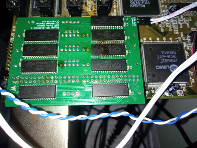
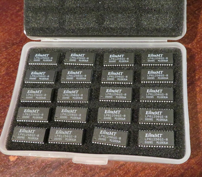
BTW: It seems I found the issue with my adapter PCB: Two of the chip select inputs are not properly soldered. I guess unmolten paste made sufficient contact when I measured it directly after assembly, but as the paste dried, the continuity broke down. For short pulses of asserting chip select (aka chip enable), capacitive coupling over the gap suffices, but if you try to keep the chip selected for some time, it starts to get deselected after some time. I'm going to include a test for that behaviour into my "UMC 8881 cache diagnostic utility" and want to verify that I can diagnose that issue before fixing the hardware. If I would run large scale production of these adapter boards, I would likely keep the broken one as test subject, but I intend to just fix and use that one instead.
Different tests I made seem to indicate that I will likely not get better than 3-2-2-2 at FSB60 with the cache chips currently soldered to that board, but possibly that gets better once the chip select pins are correctly soldered. So the "10ns" marking might be fake.