VOGONS


Asus PVI-486SP3 v.1.22 and 66MHz FSB

Topic actions

Reply 20 of 35, by debs3759

User metadata
Rank Oldbie
Rank
Oldbie
The Serpent Rider wrote on 2023-03-28, 18:02:

Only specific chipset revision has EDO support.

Which revisions support EDO? I have a 1.8 that is tested working and a 1.22 I have yet to test. It'll be a few weeks before I can get to them to check the chipset revisions

See my graphics card database at www.gpuzoo.com
Constantly being worked on. Feel free to message me with any corrections or details of cards you would like me to research and add.

Reply 22 of 35, by debs3759

User metadata
Rank Oldbie
Rank
Oldbie

Thanks

See my graphics card database at www.gpuzoo.com
Constantly being worked on. Feel free to message me with any corrections or details of cards you would like me to research and add.

Reply 24 of 35, by mkarcher

User metadata
Rank l33t
Rank
l33t
dj_pirtu wrote on 2023-03-29, 06:45:

...and my mobo has OR & OT so it means no EDO? PR is later?

Yes, indeed. "P" is after "O" in the alphabeht, and SiS used those code in alphabetical order.

Reply 25 of 35, by CoffeeOne

User metadata
Rank Oldbie
Rank
Oldbie
dj_pirtu wrote on 2023-03-21, 05:52:
Figured out yesterday that VT8228 clock chip can do 66MHz FSB so tried and it worked. […]
Show full quote

Figured out yesterday that VT8228 clock chip can do 66MHz FSB so tried and it worked.

CPU is late i486DX4/100 WB Enhanced and takes 2x66MHz=133MHz with no problems. (Tried 3x50MHz=150MHz on that QDI V4S471 but didn't make it to DOS)
Cache needs to be slowed down a little and CPU to PCI Post Write needs to be disabled or strange things will happen. If enabled and when in heavy CPU load, screen stops updating and DOS4GW gives some kind of real mode -error. When disabled it just kills PCI-speed (display card, Cirrus 5446 PCI) from 40MB/s -> 20MB/s.

My other system QDI V4S471 with CX5x86 (2x50MHz) is just as fast in memory operations, it's cache timings are fastest and memory 'faster'.

But still, that i486DX4/133 is quite fast.

Anybody else have tried 66MHz clock on this mobo?

Hello,

OK, so 66MHZ is (JP 25 to JP 28): 2-3, 2-3, 2-3, 1-2

Do you also have the 60MHz setting in your notes?

Reply 26 of 35, by feipoa

User metadata
Rank l33t++
Rank
l33t++
CoffeeOne wrote on 2023-04-30, 17:31:
Hello, […]
Show full quote
dj_pirtu wrote on 2023-03-21, 05:52:
Figured out yesterday that VT8228 clock chip can do 66MHz FSB so tried and it worked. […]
Show full quote

Figured out yesterday that VT8228 clock chip can do 66MHz FSB so tried and it worked.

CPU is late i486DX4/100 WB Enhanced and takes 2x66MHz=133MHz with no problems. (Tried 3x50MHz=150MHz on that QDI V4S471 but didn't make it to DOS)
Cache needs to be slowed down a little and CPU to PCI Post Write needs to be disabled or strange things will happen. If enabled and when in heavy CPU load, screen stops updating and DOS4GW gives some kind of real mode -error. When disabled it just kills PCI-speed (display card, Cirrus 5446 PCI) from 40MB/s -> 20MB/s.

My other system QDI V4S471 with CX5x86 (2x50MHz) is just as fast in memory operations, it's cache timings are fastest and memory 'faster'.

But still, that i486DX4/133 is quite fast.

Anybody else have tried 66MHz clock on this mobo?

Hello,

OK, so 66MHZ is (JP 25 to JP 28): 2-3, 2-3, 2-3, 1-2

Do you also have the 60MHz setting in your notes?

I couldn't find a 66 MHz option on this board, so I'd also like an answer to the above.

EDIT: JP25 yields odd results. Best to leave on 1-2.

MHz, JP26, JP27, JP28
25, 2-3, 1-2, 2-3
33, 2-3, 2-3, 1-2
40, 1-2, 1-2, 2-3
16, 2-3, 1-2, 1-2
16, 2-3, 2-3, 2-3
?, 1-2, 1-2, 1-2
50, 1-2, 2-3, 1-2
20, 1-2, 2-3, 2-3

From the above table, possibly '?' is 66 MHz and my Am5x86 just won't turn on at 3x66 at 3.6 V. For me, I really am looking for 60 MHz, which doesn't exist. I started anothre thread looking for a replacement clock generator, Replacement clock generator for Asus PVI-486SP3 to enable 60/66 MHz FSB?

Last edited by feipoa on 2023-09-26, 04:37. Edited 1 time in total.

Plan your life wisely, you'll be dead before you know it.

Reply 27 of 35, by CoffeeOne

User metadata
Rank Oldbie
Rank
Oldbie
feipoa wrote on 2023-09-23, 21:42:
I couldn't find a 66 MHz option on this board, so I'd also like an answer to the above. […]
Show full quote
CoffeeOne wrote on 2023-04-30, 17:31:
Hello, […]
Show full quote
dj_pirtu wrote on 2023-03-21, 05:52:
Figured out yesterday that VT8228 clock chip can do 66MHz FSB so tried and it worked. […]
Show full quote

Figured out yesterday that VT8228 clock chip can do 66MHz FSB so tried and it worked.

CPU is late i486DX4/100 WB Enhanced and takes 2x66MHz=133MHz with no problems. (Tried 3x50MHz=150MHz on that QDI V4S471 but didn't make it to DOS)
Cache needs to be slowed down a little and CPU to PCI Post Write needs to be disabled or strange things will happen. If enabled and when in heavy CPU load, screen stops updating and DOS4GW gives some kind of real mode -error. When disabled it just kills PCI-speed (display card, Cirrus 5446 PCI) from 40MB/s -> 20MB/s.

My other system QDI V4S471 with CX5x86 (2x50MHz) is just as fast in memory operations, it's cache timings are fastest and memory 'faster'.

But still, that i486DX4/133 is quite fast.

Anybody else have tried 66MHz clock on this mobo?

Hello,

OK, so 66MHZ is (JP 25 to JP 28): 2-3, 2-3, 2-3, 1-2

Do you also have the 60MHz setting in your notes?

I couldn't find a 66 MHz option on this board, so I'd also like an answer to the above.

JP25 only sets the PCI divisor, such that:
1-2 ==> PCI=FSB
2-3 ==> PCI = 1/2*FSB

MHz, JP26, JP27, JP28
25, 2-3, 1-2, 2-3
33, 2-3, 2-3, 1-2
40, 1-2, 1-2, 2-3
16, 2-3, 1-2, 1-2
16, 2-3, 2-3, 2-3
?, 1-2, 1-2, 1-2
50, 1-2, 2-3, 1-2
20, 1-2, 2-3, 2-3

From the above table, possibly '?' is 66 MHz and my Am5x86 just won't turn on at 3x66 at 3.6 V. For me, I really am looking for 60 MHz, which doesn't exist. I started anothre thread looking for a replacement clock generator, Replacement clock generator for Asus PVI-486SP3 to enable 60/66 MHz FSB?

Are you sure?
This is a picture from my board

PXL_20230923_223224394.jpg
Filename
PXL_20230923_223224394.jpg
File size
1.75 MiB
Views
637 views
File license
Public domain

There is a setting for 50MHz printed: 2-3, 2-3, 1-2, 2-3
So JP 26, 27, 28 is 2-3, 1-2, 2-3. It is the same as for 25MHz. According to your theory, that would be 25MHz with a PCI clk of 12.5MHz. No, you are wrong, that is a setting for 50MHz.
I am pretty sure that (JP 25 to JP 28): 2-3, 2-3, 2-3, 1-2 IS FSB 66MHz.

Reply 28 of 35, by CoffeeOne

User metadata
Rank Oldbie
Rank
Oldbie
CoffeeOne wrote on 2023-09-23, 22:46:
Are you sure? This is a picture from my board PXL_20230923_223224394.jpg There is a setting for 50MHz printed: 2-3, 2-3, 1-2, 2- […]
Show full quote
feipoa wrote on 2023-09-23, 21:42:
I couldn't find a 66 MHz option on this board, so I'd also like an answer to the above. […]
Show full quote
CoffeeOne wrote on 2023-04-30, 17:31:

Hello,

OK, so 66MHZ is (JP 25 to JP 28): 2-3, 2-3, 2-3, 1-2

Do you also have the 60MHz setting in your notes?

I couldn't find a 66 MHz option on this board, so I'd also like an answer to the above.

JP25 only sets the PCI divisor, such that:
1-2 ==> PCI=FSB
2-3 ==> PCI = 1/2*FSB

MHz, JP26, JP27, JP28
25, 2-3, 1-2, 2-3
33, 2-3, 2-3, 1-2
40, 1-2, 1-2, 2-3
16, 2-3, 1-2, 1-2
16, 2-3, 2-3, 2-3
?, 1-2, 1-2, 1-2
50, 1-2, 2-3, 1-2
20, 1-2, 2-3, 2-3

From the above table, possibly '?' is 66 MHz and my Am5x86 just won't turn on at 3x66 at 3.6 V. For me, I really am looking for 60 MHz, which doesn't exist. I started anothre thread looking for a replacement clock generator, Replacement clock generator for Asus PVI-486SP3 to enable 60/66 MHz FSB?

Are you sure?
This is a picture from my board PXL_20230923_223224394.jpg
There is a setting for 50MHz printed: 2-3, 2-3, 1-2, 2-3
So JP 26, 27, 28 is 2-3, 1-2, 2-3. It is the same as for 25MHz. According to your theory, that would be 25MHz with a PCI clk of 12.5MHz. No, you are wrong, that is a setting for 50MHz.
I am pretty sure that (JP 25 to JP 28): 2-3, 2-3, 2-3, 1-2 IS FSB 66MHz.

Here are more settings: I think you were also particpating in this thread:
Re: Test:486 undocumented jumper settings

Reply 29 of 35, by feipoa

User metadata
Rank l33t++
Rank
l33t++

I could be wrong about JP25 being the PCI divisor. It could be the S3 input. I will need to run some tests with the scope to be certain.

Here is the result from my 50 MHz setting, which 5u3 calls a 48 MHz setting. chkcpu also calls it 50 MHz.

IMG_2557.JPG
Filename
IMG_2557.JPG
File size
86.97 KiB
Views
609 views
File license
CC-BY-4.0
IMG_2558.JPG
Filename
IMG_2558.JPG
File size
109.22 KiB
Views
609 views
File license
CC-BY-4.0

Plan your life wisely, you'll be dead before you know it.

Reply 30 of 35, by Horun

User metadata
Rank l33t++
Rank
l33t++

I think jp25 changes the cpu clock from CLK to CLK*2, so for 50Mhz jp25 would be changed while 26-28 remain the same.... note how the jumpers on the sticker are same for 25Mhz as 50Mhz except jp25.
The datasheet for AV9155-02 shows a CLK out pin and a CLK*2 out pin (called CPU and 2x CPU)...and no 30mhz according to the table.....it also has a BUSCLK output of 32Mhz which probably goes to PCI and a /4 for ISA...
assuming the VT8228 is similar (since the jumpers are hardwired) in config....and the VT8225 also has a 1x and 2x clock set by S3.....just observations... 😀

Hate posting a reply and then have to edit it because it made no sense 😁 First computer was an IBM 3270 workstation with CGA monitor. Stuff: https://archive.org/details/@horun

Reply 31 of 35, by feipoa

User metadata
Rank l33t++
Rank
l33t++

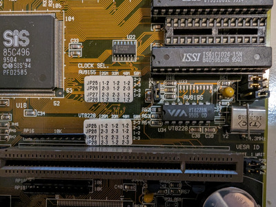
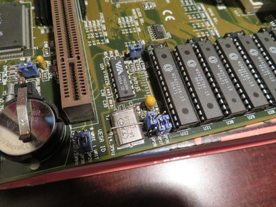
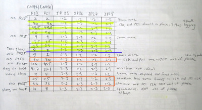
My board is revision 1.8 and it doesn't have any silkscreen or stickers indicating how 50 MHz jumpers would set. I have run all possible jumper combinations for JP25, 26, 27, 28. I measured CLK directly at the CPU's CLK pin, I measured PCI CLK from the PCI slot. The results are attached.

Asus_PVI_486SP3_complete_clk_gen_table.JPG
Filename
Asus_PVI_486SP3_complete_clk_gen_table.JPG
File size
145.6 KiB
Views
582 views
File license
CC-BY-4.0

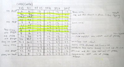
The entries I highlighted in yellow are the ones which I believe are the correct and operational. All others are, non-functional, except for a second 25 MHz setting with a bumpy waveform.

The theory that the VIA PLL follows the convention of the AV9155 PLL seems sound, however the measured results don't follow this CLK*2 convention. The exception is for the 50 MHz setting, which on my board is:

50 MHz FSB
JP25, JP26, JP27, JP28
1-2, 1-2, 2-3, 1-2

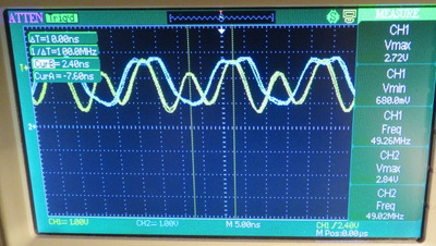
If we adjust JP25 to 2-3, we'd expect the 50 MHz setting to double, which it does, but only for the 50 MHz setting.

Thus,
JP25, JP26, JP27, JP28
2-3, 1-2, 2-3, 1-2
has the following waveform, but is NO POST:
Yellow is CPUCLK, blue is PCI CLK.

100MHz.JPG
Filename
100MHz.JPG
File size
124.72 KiB
Views
572 views
File license
CC-BY-4.0

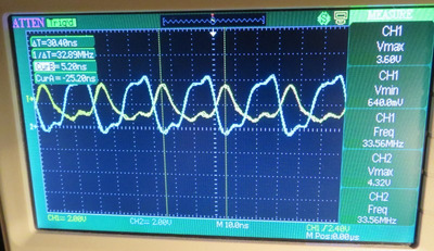
From this analogy, we might expect the 33 MHz setting, with JP25 set to 2-3 to be the 66 MHz setting, but alas, it is not. It is still 33 MHz and no POST. For the most part, when JP25 is set to 2-3, the PCI CLK and CPU CLK are 180 degrees out of phase. All but one setting with JP25 set to 2-3 would not POST (the other being the second 25 Mhz FSB setting with bumpy waveform).

Last edited by feipoa on 2023-09-24, 02:41. Edited 3 times in total.

Plan your life wisely, you'll be dead before you know it.

Reply 32 of 35, by feipoa

User metadata
Rank l33t++
Rank
l33t++

This is what the proposed 66 MHz setting looks like. FSB CLK is yellow. PCI CLK is blue.

Bogus_66Mhz_FSB_1.JPG
Filename
Bogus_66Mhz_FSB_1.JPG
File size
138.02 KiB
Views
578 views
File license
CC-BY-4.0
Bogus_66Mhz_FSB_2.JPG
Filename
Bogus_66Mhz_FSB_2.JPG
File size
121.16 KiB
Views
578 views
File license
CC-BY-4.0

It is still 33 MHz on my system, with asymmetric widths for the peaks/valleys. Does this work at 66 Mhz on your system? Could you provide a scope image?

Plan your life wisely, you'll be dead before you know it.

Reply 33 of 35, by feipoa

User metadata
Rank l33t++
Rank
l33t++

I have confirmed that JP25 pin 3 is the CLK*2 pin on the PLL (both VT8228N and AV9155). It is unclear why I am not witnessing 2x clocks on the scope or when running the motherboard.

Plan your life wisely, you'll be dead before you know it.

Reply 34 of 35, by Horun

User metadata
Rank l33t++
Rank
l33t++

wow yeah something is screwy !! Can you recheck those I boxed in red ? Most of those with jp25 @ 2-3 are FSB to PCI 2:1 but not those....
added: in your chart the 100Mhz is close 2 to 1, makes no sense that the 25 and 33 are not....if the timer can do 100Mhz makes no sense it can not do 50 or 66...

Attachments

Hate posting a reply and then have to edit it because it made no sense 😁 First computer was an IBM 3270 workstation with CGA monitor. Stuff: https://archive.org/details/@horun

Reply 35 of 35, by feipoa

User metadata
Rank l33t++
Rank
l33t++

Refer to above oscilloscope image titled, Bogus_66Mhz_FSB_2.JPG. It is really at 33 MHz. Similarly, I looked at the scope image for the other two configurations you've outlined in orange.

Plan your life wisely, you'll be dead before you know it.