VOGONS


First post, by RockstarRunner

User metadata
Rank Member
Rank
Member

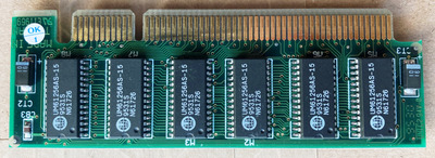
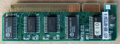
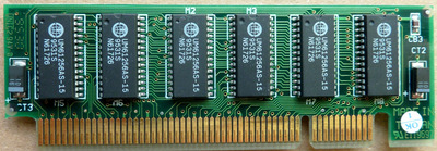
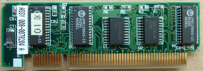
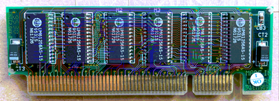
The proprietary cache module, used by the 486-GAC-2 and some other boards has been reverse engineered, and is now available as an open source project that you can make for yourself if you happen to have one of the compatible systems.
This finally helps out owners of these boards, where original modules are essentially unobtanium.
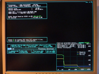
Adding the cache module, when properly configured, can take a DX4 100 running Doom max details time demo from 29.8 fps to 37.2 fps, an increase of almost 25%

I would like to thank:-
Rasz_pl for reverse engineering the module, and creating the PCB design.
Majestyk for providing information from his very rare original module.
Miisalo for debugging and soldering work.
(I did some stuff too, but those guys are the mvp's)

You can find the project, Gerbers and information needed to locate parts from here:
Open Source AT&T Globalyst/NCR/FIC 486-GAC-2 proprietary Cache Module reproduction

Give this whole thread a read, if you want to see an interesting journey of discovery, face palms and eventual triumph.

Note: I have parts left for two modules, if someone needs, either assembled or kit form. P.M. for details.

*** Original post below ***

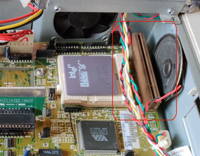
So i've gone back to playing with my 486 Pizza Box PC, a Globalyst 510 with an FIC 486-GAC-2 motherboard.
As a few people on this forum are aware, this board has a proprietary cache module slot, that resembles a VLB connector.
So far, no one who has mentioned they have been looking for cache modules for this board, has found one that works, at best, they fit but are not compatible.

486gac2_cache_slot.jpg
Filename
486gac2_cache_slot.jpg
File size
462.45 KiB
Views
1803 views
File license
Fair use/fair dealing exception

I'd really like to complete this PC, and add a cache module, so I turn to you, the detectives of Vogons, to help solve the mystery of this cache module.

As far as is understood, it is quite likely an async SRAM cache module.
I've read a document describing it as "optional 256KB write-back second level cache".

In this thred, user Niezgodka apparently has a machine with cache module, and sent image privately to user lazibayer, but that's all we can learn from that.
Perfect 486 PC, but ugly Bios and slow RAM :(

Another thread with user lazibayer trying different modules, without success.
Re: need some help finding correct L2 cache RAM

This page has a Globalyst 510 in testing, and shows a cache module.
https://www.high-voltage.cz/2018/globalyst-51 … kolo-vylepseni/
From what I can make out from the pictures, I think it says:
MODEL: CACHE MODULE
DOC: 13630
Only the labels of two chips can be read, and one (tag?) is covered by a sticker.
I have searched eBay countless times with that ID, and never turned up anything.

Heck, If we could even get detailed pictures of both sides of a known working module, it might lead to possibilities regarding creating a reproduction.
Yeah, I know this is a shot in the dark, but if any forum would know, it's this one.

Last edited by RockstarRunner on 2024-04-20, 12:30. Edited 5 times in total.

Reply 1 of 119, by majestyk

User metadata
Rank Oldbie
Rank
Oldbie

I own only one of these modules. It´s a 256K L2 cache module with integrated buffer circuits and a proprietary pinout.

256K_prop1.JPG
Filename
256K_prop1.JPG
File size
1.26 MiB
Views
1793 views
File license
Fair use/fair dealing exception
256K_prop2.JPG
Filename
256K_prop2.JPG
File size
1.28 MiB
Views
1793 views
File license
Fair use/fair dealing exception
P1220275.JPG
Filename
P1220275.JPG
File size
636.12 KiB
Views
1419 views
File license
Fair use/fair dealing exception
P1220276.JPG
Filename
P1220276.JPG
File size
556.7 KiB
Views
1419 views
File license
Fair use/fair dealing exception

To make things worse, FIC sold two different versions with different pinouts (and the same "VLB"-socket). Only the one in the pictures works on a 486-GAC2 and a few other FIC mainboards.

When you add the cache module, the 3.3V VRM module and a AMD 5x86 the performance is quite impressive compared to the original configuration.

Last edited by majestyk on 2023-09-14, 14:02. Edited 1 time in total.

Reply 2 of 119, by RockstarRunner

User metadata
Rank Member
Rank
Member

Wow, ok, didn't expect someone to actually have one. Thanks for sharing.

So, at least it is clear that there is nothing proprietary about the chips used, some ram & buffers, so that's good news I suppose.

One day maybe my ebay saved search will ping something, not that it has for some years now 🤣

Reply 3 of 119, by RockstarRunner

User metadata
Rank Member
Rank
Member

As difficult as the task may be, I have started to map the traces from the pictures you provided, at least those that don't end somewhere under a chip.

@majestyk
Would you be able to take a few more pictures, some sightly angled maybe, to make the shadowed areas clearer?
And do you have a multimeter?
Once I've mapped everything I am able to, it would be greatly beneficial if you could confirm my findings, and help map the traces that are under the chips.
I've discussed this with my electronics expert friend, and he doesn't see any reason a repro can't be made, with some effort.

Reply 4 of 119, by majestyk

User metadata
Rank Oldbie
Rank
Oldbie

I will take some more detailed pictures.
I could also could do some measuring to identify the ground and Vcc pins and check for continuity between all the I/O, address, CS, CE pins at each SRAM and buffer chip and the pins of the "VLB"-socket.
This will probably not reveal all the information like the number of layers, or traces that connect chips with each other.

Reply 8 of 119, by rasz_pl

User metadata
Rank l33t
Rank
l33t

I have a feeling you will need to attack it from both directions. Take out the mobo and map this slot pinout to chipset.
next find another board with same chipset and onboard cache sockets https://theretroweb.com/motherboards/?chipset … 85&showImages=1 to complete the map
chipset datasheet pinout page 30
https://datasheet.datasheetarchive.com/origin … DSA00204677.pdf
https://dosdays.co.uk/media/via/VIA_82C496G.pdf

Open Source AT&T Globalyst/NCR/FIC 486-GAC-2 proprietary Cache Module reproduction

Reply 9 of 119, by majestyk

User metadata
Rank Oldbie
Rank
Oldbie

I added two pictures above after cleaning the stick.

rasz_pl, do VT82C486A and VT82C496G share the same pinout?

I have most of the FIC mainboards with this chipset here, so I could do the measuring. The two 244 buffer chips are on the cache-stick here - we need to measure between the chipset and the buffer inputs in this case.

If the L2 cache stick is present and you do a few little mods, you can run an AMD 5x86 @133 MHz in L1 cache Write Back mode. And that´s quite a progress for a mainboard that was usually equipped with a SX33 CPU...

P1220278c.JPG
Filename
P1220278c.JPG
File size
136.96 KiB
Views
1408 views
File license
Public domain
P1220281c.JPG
Filename
P1220281c.JPG
File size
743.05 KiB
Views
1406 views
File license
Public domain

Reply 10 of 119, by rasz_pl

User metadata
Rank l33t
Rank
l33t
majestyk wrote on 2023-09-14, 14:07:

rasz_pl, do VT82C486A and VT82C496G share the same pinout?

I didnt spot the number difference when searching and "helpful" google decided to ignore quotations marks 🙁. NVM then 😀

Open Source AT&T Globalyst/NCR/FIC 486-GAC-2 proprietary Cache Module reproduction

Reply 11 of 119, by RockstarRunner

User metadata
Rank Member
Rank
Member

Why did I stop receiving notifications about posts to this thread!? Life got in the way, but I'm trying to find time to get back to this cache project.
Best I could do now, is pull the motherboard, and see where the traces go from the cache socket.
As for 'getting these made', I wouldn't hold my breath, this wouldn't be easy even if I knew what I was doing (not an electrical engineer, just stubborn and happen to know someone who could help me get a pcb designed, if I can gather enough information)

This insanity represents where I got to last time I looked at this

256K_prop1.png
Filename
256K_prop1.png
File size
800.17 KiB
Views
1007 views
File license
Fair use/fair dealing exception

Red lines are traces I was thinking were likely, Pink lines are traces I was uncertain about or couldn't see where they end
Cyan lines are the same as red, but the other side of the pcb, Blue lines are same category as Pink, but again for the other side.
Numbers are vias (for both sides)..... so, pretty worthless , but was at least a mind excercise for me

Reply 12 of 119, by rasz_pl

User metadata
Rank l33t
Rank
l33t

Great job tracing those lines. Picture isnt the best medium for this. Personally I couldnt figure out your number scheme so did it from scratch myself 🙁 Try Kicad, it looks intimidating but really isnt https://www.youtube.com/watch?v=3FGNw28xBr0

> but was at least a mind excercise for me
Sooo instead of playing Into the Breach yesterday 😜 I made a you this preliminary project. Footprint are wrong (need to make/find real SOJ 28L and proper edge connector, now its just butchered PCI 😜) and there is still a ton to missing vias/traces/connections to fix/guess (~200 errors/warnings), I just went sleepy 😜 will probably continue tomorrow.

Attachments

Open Source AT&T Globalyst/NCR/FIC 486-GAC-2 proprietary Cache Module reproduction

Reply 13 of 119, by RockstarRunner

User metadata
Rank Member
Rank
Member

Wow, what an effort, thanks!
That picture, I actually have it in Photoshop, with a bunch of layers, were it is more 'readable', and true it's certainly not the best format for this, but it was all I knew to get started. The numbers for the vias are just sequential as I labelled them, so it was 'easier' to understand when flipping the side of the module, where traces were connected.

Those traces and vias that go under chips are frustrating, as there isn't any good way to be sure where they go.

I'll look in to setting up kicad as you suggested. Thanks again for the effort.

Reply 14 of 119, by rasz_pl

User metadata
Rank l33t
Rank
l33t

Some of the traces under chips are easy to guess once you connect everything else, as in only one pad left 😀 others can be guessed by examining function. Still I think there will be a point around 99% where only majestyk will be able to help with his original module and a multimeter to validate guesses, and maybe peeling that sticker 😀 Of course desoldering would solve all problems, but where is the fun in that :]

Open Source AT&T Globalyst/NCR/FIC 486-GAC-2 proprietary Cache Module reproduction

Reply 15 of 119, by RockstarRunner

User metadata
Rank Member
Rank
Member

Desoldering would lay this thing bare, but I would not and will not ask anyone with one of these modules to potentially damage it by doing so, they're too rare. And yes, imagine the sense of accomplishment to pull this off without resorting to that.

I installed KiCAD, and opened your project, wow, I can see I have a lot of learning to do, you weren't kidding that it looks intimidating
p.s. rasz_pl I sent you a PM, but it's stuck in outbox

Reply 16 of 119, by rasz_pl

User metadata
Rank l33t
Rank
l33t

First look at your trace image and I already spotted few mistakes in my work 😀 for example I made R6 go somewhere else. Goes to show two pairs of eyes are better than one! makes perfect sense now with via used for M2 power.

Most basic kicad tips: Open sram.kicad_pro first, that way PCB and schematic will be logically linked while working on them. Ctrl-Tab flips between front and back view in PCB viewer, to flip board horizontally you can either click checkbox in lower right corner or go to Preferences and make keyboard shortcut. You cant just draw connections in PCB viewer, you need to first make those in Schematic editor, then F8 to propagate changes to PCB editor.
Ill make github repository for the project. With majestyk pictures and retroweb pictures of
FIC 486-GAC-V
FIC 486-GIO-VP
FIC 486-GIO-VT
FIC 486-GIO-VT2
FIC 486-GT
FIC 486-GVT
FIC 486-GVT-2
we should have everything needed. Its like a puzzle and once you fill enough knowns the unknowns become quite obvious. Ironically I think power and ground on the cache connector itself are the only things I wont be able to deduce from images, every 4th pin is a ground stich, but might be power.

Open Source AT&T Globalyst/NCR/FIC 486-GAC-2 proprietary Cache Module reproduction

Reply 17 of 119, by RockstarRunner

User metadata
Rank Member
Rank
Member

Yeah, GitHub is a great idea.
Thanks for the starter advice, after looking through the project you linked, I decided I would try to do a really simple starter project, to help learn some basics.

Reply 19 of 119, by rasz_pl

User metadata
Rank l33t
Rank
l33t
RockstarRunner wrote on 2024-02-05, 07:48:
rasz_pl wrote on 2024-02-05, 01:56:

Its like a puzzle and once you fill enough knowns the unknowns become quite obvious.

So it's Return of the Obra Dinn 😆

or excellent 'The Case of the Golden Idol' 😀 https://github.com/raszpl/FIC-486-GAC2-Cache-Module
Still couple errors and ~200 warnings (unconnected traces/vias). One thing im struggling right now is A4, cant find a way it would be connected under the chips. Most obvious way Is right there between Chips M3 and M7. M7 pin 10 has clear way to a via next to M3, but there is no trace on pictures 😮 what the hell hehe.

Do you have motherboard handy to do some measurements? Would be nice to verify ground/power connections on cache slot.
Another bigger task is downloading socket 3 168-Pin PGA pinout (for example https://www.retrobrewcomputers.org/lib/exe/fe … types_12203.pdf) and going over all CPU Address/data A2-31 D0-31 lines sticking a needle in socket and measuring where it goes on the cache slot.

Open Source AT&T Globalyst/NCR/FIC 486-GAC-2 proprietary Cache Module reproduction