VOGONS


Reply 20 of 119, by majestyk

User metadata
Rank Oldbie
Rank
Oldbie

Using the common numbering for VLB slots
Ground is at pins
A1, A5, A9, A13, A17, A21, A25, A29, A33, A37, A41, A45, A50, A54
B3, B23, B27, B35, B43, B52

5V (Vcc) is at pins
B7, B11, B15, B19, B31, B39, B48, B56

The data lines:
CPU - Cache-Slot pin
D0-B1
D2-B4
D9-B13
D11-B16
D19-B26
D20-B28
D1-B2
D6-B9
D5-B8
D3-B5
D8-B12
D13-B18
D18-B25
D21-B29
D22-B30
D4-B6
D7-B10
D14-B20
D16-B22
D12-B17
D15-B21
D10-B14
D17-B24
D23-B32
D27-B37
D25-B34
D24-B33
D26-B36
D28-B38
D31-B42
D29-B40
D30-B41

Last edited by majestyk on 2024-02-05, 17:20. Edited 2 times in total.

Reply 21 of 119, by RockstarRunner

User metadata
Rank Member
Rank
Member

I would have to extract the motherboard from the case, which will take a little while (very tightly packed, and I squeezed an Orpheus II in to it, which will need to be removed carefully), but I can do that, if it helps.

...

Yep, now I remember what a struggle it was to fit that card in there

IMG20240205185851.jpg
Filename
IMG20240205185851.jpg
File size
523.77 KiB
Views
449 views
File comment
Extracted board
File license
Fair use/fair dealing exception

Now I'll go find my multimeter, so I can "going over all CPU Address/data A2-31 D0-31 lines sticking a needle in socket and measuring where it goes on the cache slot."

Reply 23 of 119, by RockstarRunner

User metadata
Rank Member
Rank
Member

Back of the PCB, shows some of the traces at least

IMG20240205193123.jpg
Filename
IMG20240205193123.jpg
File size
896.66 KiB
Views
434 views
File comment
Back of CPU cache
File license
Fair use/fair dealing exception

It looks like Majestyk has already done the D's, I am working on the A's but it's bit slow progress, bear with me...

Reply 24 of 119, by RockstarRunner

User metadata
Rank Member
Rank
Member

I measured the traces from A2 to A31 from the back of the board to the cache slot, and found these connections

CPU_Cache_Address_Lines_crop.png
Filename
CPU_Cache_Address_Lines_crop.png
File size
486.74 KiB
Views
424 views
File comment
address_lines
File license
Fair use/fair dealing exception

RED = Connected to cache socket
PINK = No connection (that I found)

I'm not yet certain what pins those are according to VLB mapping, I think it's this:
CPU - CACHE
A5 - A20
A6 - A19
A7 - A18
A8 - A16
A9 - A15
A10 - A14
A11 - A12
A12 - A11
A13 - A6
A14 - A8
A15 - A7
A16 - A10
A17 - A4

(rasz_pl, the full rez versions are in the share folder, if you need them)

Last edited by RockstarRunner on 2024-02-05, 19:40. Edited 4 times in total.

Reply 25 of 119, by rasz_pl

User metadata
Rank l33t
Rank
l33t

Cache has two banks, and now Im struggling with chip M6 which should be in second bank, but I cant find any other way of routing its OE/CE signals but to M2, except they also share data pins so its impossible 😀 oh what fun. Down to ~80 unrouted signals. Ill look at the readings you got now to validate my data/address guesses.

edit: first problem, I numbered slot other way around 😁 debating if I want to change it 😀

>5V (Vcc) is at pins
>B7, B11, B15, B19, B31, B39, B48, B56

What about B3? has short thick track going to a power stich like the rest of them.

>The data lines:

I think I got that right by just guessing, will have to rename slot pins to be sure.

Open Source AT&T Globalyst/NCR/FIC 486-GAC-2 proprietary Cache Module reproduction

Reply 27 of 119, by majestyk

User metadata
Rank Oldbie
Rank
Oldbie
rasz_pl wrote on 2024-02-05, 19:18:

>5V (Vcc) is at pins
>B7, B11, B15, B19, B31, B39, B48, B56

What about B3? has short thick track going to a power stich like the rest of them.

B3 is definitely ground - just like in my list.

Reply 28 of 119, by rasz_pl

User metadata
Rank l33t
Rank
l33t
majestyk wrote on 2024-02-05, 19:37:

B3 is definitely ground - just like in my list.

I looked at first row and somehow missed the second one, sorry

>A13
>A16

the only two swapped address lines! FIC even managed to keep data lines in order without swapping 😮
github updated, got it down to 3 errors, 76 warnings.
Edit1:Main problem now is is M6. majestyk are pins 22 of M6 and M2 connected? nvm I hallucinated a track like a bad AI
Edit2: Attached progress, about 80% there. DRC zero errors, down to 62 violations - dangling vias/tracks waiting to be connected. Still bad footprints and I havent gotten around to fixing power/ground pins. Whats left is figuring LS244 address buffering mapping, TAG ram address and output pins to edge mapping, WE/CE/OE mapping to edge.

Attachments

Open Source AT&T Globalyst/NCR/FIC 486-GAC-2 proprietary Cache Module reproduction

Reply 29 of 119, by majestyk

User metadata
Rank Oldbie
Rank
Oldbie

I did some measuring at the TAG chip (MD1) today:

32Kx8_pinout.JPG
Filename
32Kx8_pinout.JPG
File size
17.06 KiB
Views
331 views
File license
Public domain

Both OE# and CE# are grounded.

MD1 pin -> VLB connector pin
WE -> A55
I/O0 -> A39
I/O1 -> A40
I/O2 -> A42
I/O3 -> A43
I/O4 -> A44
I/O5 -> A48
I/O6 -> A49
I/O7 -> A51

A0 -> A6 (and pin 6 of U1) [via R3 = 0 Ohm, if R4 was populated instead it would pull A0 up]
A1 -> A22 (and pin 4 of U1)
A2 -> A20 (and pin 11 of U1)
A3 -> A19 (and pin 13 of U1)
A4 -> A18 (and pin 15 of U1)
A5 -> A16 (and pin 17 of U1)
A6 -> A15 (and pin 8 of U2)
A7 -> A14 (and pin 6 of U2)
A8 -> A12 (and pin 4 of U2)
A9 -> A11 (and pin 2 of U2)
A10 -> A10 (and pin 11 of U2)
A11 -> A8 (and pin 13 of U2)
A12 -> A7 (and pin 15 of U2)
A13 -> Vcc
A14 -> A4 (and pin 17 of U2) [via R1 = 0 Ohm, if R2 was populated instead it would pull A14 up]

rasz, do you need any info about WE/CE/OE of the cache banks?

Reply 30 of 119, by rasz_pl

User metadata
Rank l33t
Rank
l33t
majestyk wrote on 2024-02-06, 08:42:

I did some measuring at the TAG chip (MD1) today:

Fantastic! Some of those are easy to guess, some really hard, and a few quite impossible (I have a feeling TAG output order is really critical for example) without digging into VIA chipset datasheets looking for something VT82C486A related.

Edit: Just did TAG chip outputs, turns out there was only one way they all fit and I already got it 99% of the way in previous upload with under_tag8-11 almost touching correct Tag Q pads 😮

majestyk wrote on 2024-02-06, 08:42:

Both OE# and CE# are grounded.

I dug into my collection of motherboard schematics and found few with async cache, all had both grounded for TAG chip. This project is a great opportunity to get more intimate with x86 cache implementations 😀

majestyk wrote on 2024-02-06, 08:42:

WE -> A55

damn, dont know how to route that yet :] the only logical place goes above U1, under M6, and ends up under U2 😀 It will get to me eventually once more unknowns are removed, maybe under M4.

majestyk wrote on 2024-02-06, 08:42:
A0 -> A6 (and pin 6 of U1) [via R3 = 0 Ohm, if R4 was populated instead it would pull A0 up] A1 -> A22 (and pin 4 of U1) A2 -> […]
Show full quote

A0 -> A6 (and pin 6 of U1) [via R3 = 0 Ohm, if R4 was populated instead it would pull A0 up]
A1 -> A22 (and pin 4 of U1)
A2 -> A20 (and pin 11 of U1)
A3 -> A19 (and pin 13 of U1)
A4 -> A18 (and pin 15 of U1)
A5 -> A16 (and pin 17 of U1)
A6 -> A15 (and pin 8 of U2)
A7 -> A14 (and pin 6 of U2)
A8 -> A12 (and pin 4 of U2)
A9 -> A11 (and pin 2 of U2)
A10 -> A10 (and pin 11 of U2)
A11 -> A8 (and pin 13 of U2)
A12 -> A7 (and pin 15 of U2)
A14 -> A4 (and pin 17 of U2) [via R1 = 0 Ohm, if R2 was populated instead it would pull A14 up]

I got most of those very close but slightly wrong, like swapped A11 A12. I think those were guessworks where two vias go under sram and you have to randomly pick if track goes above or below a via.

majestyk wrote on 2024-02-06, 08:42:

rasz, do you need any info about WE/CE/OE of the cache banks?

Those go into A44-58, but cant tell order yet because of the sticker on your module 😀 Leave it for now, I want to see if it I can guess it, for example Im fairly sure M4/M8 common WE goes to B50/55.
Thank you for great help!

Last edited by rasz_pl on 2024-02-06, 11:13. Edited 2 times in total.

Open Source AT&T Globalyst/NCR/FIC 486-GAC-2 proprietary Cache Module reproduction

Reply 31 of 119, by RockstarRunner

User metadata
Rank Member
Rank
Member

Yeah! Great work, both of you.
I guess there isn't anymore I can do with my board that would be useful, so if that's the case, I'll put everything back.

Think I need to start hunting for ram chips to build prototypes, when things get to that stage.

Reply 32 of 119, by rasz_pl

User metadata
Rank l33t
Rank
l33t

Look into what is available and cheap, feipoa seems to have a good grasp on availability of old stock srams Re: Lets make new M919 Cache sticks? Footprints are important. I still didnt bother to change to correct one, whats on the pcb is I think slightly too wide, Ill be fixing it later.

Open Source AT&T Globalyst/NCR/FIC 486-GAC-2 proprietary Cache Module reproduction

Reply 33 of 119, by rasz_pl

User metadata
Rank l33t
Rank
l33t

Progress attached, 0 errors 18 warnings. Just a couple tracks left.

>I got most of those very close but slightly wrong, like swapped A11 A12. I think those were guessworks where two vias go under sram and you have to randomly pick if track goes above or below a via.

scratch that, I got all the address lines going to U1 U2 right last time 😮 I just misunderstood your pin assignment report wrong, too many A0 a0 confused me 😀 Lovely puzzle.

Attachments

Open Source AT&T Globalyst/NCR/FIC 486-GAC-2 proprietary Cache Module reproduction

Reply 34 of 119, by rasz_pl

User metadata
Rank l33t
Rank
l33t
RockstarRunner wrote on 2023-06-05, 15:50:
This page has a Globalyst 510 in testing, and shows a cache module. https://www.high-voltage.cz/2018/globalyst-51 … kolo-vylepse […]
Show full quote

This page has a Globalyst 510 in testing, and shows a cache module.
https://www.high-voltage.cz/2018/globalyst-51 … kolo-vylepseni/
From what I can make out from the pictures, I think it says:
MODEL: CACHE MODULE
DOC: 13630
Only the labels of two chips can be read, and one (tag?) is covered by a sticker.

So I missed this somehow the first time. Image:

globalyst-510-02-1.jpg
Filename
globalyst-510-02-1.jpg
File size
269.41 KiB
Views
251 views
File license
Fair use/fair dealing exception

Its routed slightly differently. At first I assumed I made a mistake and started correcting pcb :--) then thankfully sanity checked with majestyk provided images 😀
U1 pin 1 has Via almost in a pad, 3 and 16 have new connections straight to via.
5 vias under U2 silkscreen arent in line but a C shape, and finally U2 pins 19 and 20 again almost Via almost in a pad instead of going up.
Mind you those are only a routing differences, Imo connections re the same, someone just played with placement. Very weird, usually you wouldnt touch something like that.

Open Source AT&T Globalyst/NCR/FIC 486-GAC-2 proprietary Cache Module reproduction

Reply 35 of 119, by majestyk

User metadata
Rank Oldbie
Rank
Oldbie

There´s also a second variant of this "VLB" cache stick for the AT&T Globalyst 550.
It´s pinout / layout is completely different. Care must be taken not to mix up the 2 versions.

ATT-Globalyst_550.jpg
Filename
ATT-Globalyst_550.jpg
File size
79.44 KiB
Views
245 views
File license
Public domain

Reply 36 of 119, by rasz_pl

User metadata
Rank l33t
Rank
l33t

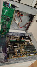
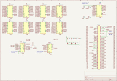
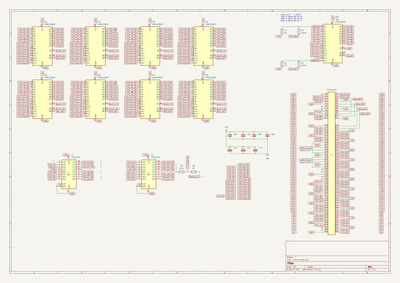
I ran out of things to route based on placement of tracks on pcb. What is left is logical deduction. Looking at the diagram there are some things that confuse me.
I understand R1 R2 limiting TAG ram addressability with smaller cache.
I somewhat understand R5 R6 linking last cache address bit to second bank thus switching from 2 bank arrangement to single.
What I dont understand is what is happening with R3 R4. What would be the point of cutting off CPU_A13? Wouldnt unpopulated R3 leave uncached holes? or worse broken cache every 16KB as cache not seeing CPU_A13 couldnt distinguish real addresses? ... wait a minute, its not CPU_A13!! 😁 looking few posts earlier

>>A13
>>A16
>the only two swapped address lines!

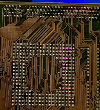
FIC didnt swap those after all! RockstarRunner how could you? top 10 anime betrayals! :] A13 is Q-10, A16 Q-9, after swapping A13 A16 back R3 R4 makes perfect sense, I think this is allowing using much cheaper 8KB chips. This made me look at your picture more closely, there is in fact bottom layer track between CPU A4 and cache slot a22 just like I guessed there would be in the diagram called under_U1_1 😀 lovely, so address bus is 100% correct.

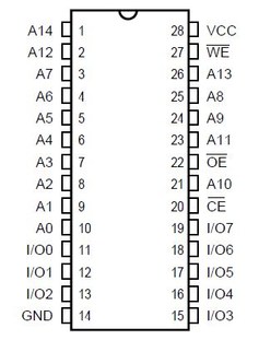
I think this is the final resistor function description (not 100%, still needs validating):
Cache size:___________| Populate 0ohm:
256K (2 banks, 8x32KB)| R1 R3 R5
128K (1 bank, 4x32KB) | R2 R3 R6
64KB (2 banks, 8x8KB) | R2 R4

I wonder what the real world difference there is between those three, especially between 4x32KB vs 8x8KB. Hope RockstarRunner tests it if we manage to finish this project successfully.

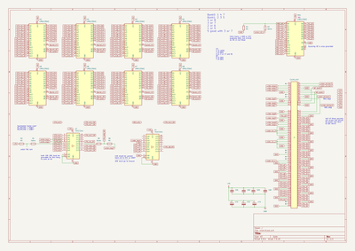
Im tapped out at the moment. Attaching progress. 0 errors, 7 Warnings. 5 connections missing, 11 guesses and assumptions on U1 U2 and some more on common lines.
Majestyk could you please check some things for me?
- U1 2? I have no idea where it could be connected to
- U1 3 to M1 5?
- U1 7 to M1 7?
- U1 9 to M1 8?
- U1 14 to M1 26? is it connected to VIA right above U1?
- U1 16 to M1 9?
- are all M1-M8 pin 10s connected together? This doesnt make sense logically, I have a feeling it should be split into groups M1-M4 and M5-M8.
- U1 18 to M1 10 or M5 10?

- U2 12 to m1 4? is it connected to VIA right above U2?
- U2 14 to M1 3?
- U2 16 to M1 25?

-cache slot a28 a30-a32 to a56 or a57? I wonder why so many connections bundled together
-cache slot a34-a36 a38 to a57 or a56? I wonder why so many connections bundled together
-cache slot a56 to M8 20?
-cache slot a57 to M4 20?
-cache slot b57 to M8 22?
-cache slot b58 to M3 22?

-cache slot b55 to M8 M4 27?
-cache slot b54 to M7 M3 27?
-cache slot b53 to M6 M2 27?
-cache slot b51 to M5 M1 27?

I thinks thats all, this might be the final stretch.

Attachments

Open Source AT&T Globalyst/NCR/FIC 486-GAC-2 proprietary Cache Module reproduction

Reply 37 of 119, by RockstarRunner

User metadata
Rank Member
Rank
Member

"FIC didnt swap those after all! RockstarRunner how could you? top 10 anime betrayals! :] "
I don't understand, I thought I was being careful when testing the connectivity. Did I just get the slot pin wrong, or the mapping?
I'd check it again, but I put the damn pc back together again, which is a big pain. I mean I would, but you seem to have resolved the issue anyway.

"I wonder what the real world difference there is between those three, especially between 4x32KB vs 8x8KB. Hope RockstarRunner tests it if we manage to finish this project successfully."
I'm not sure anyone would want less than 256k if they were making one of these, but perhaps main issue is having to order even more chips, and cost starts to mount up. At least 128k is testable with same chip order. I'll at least have a look for 8k chips.

Reply 38 of 119, by rasz_pl

User metadata
Rank l33t
Rank
l33t
RockstarRunner wrote on 2024-02-08, 07:28:

I don't understand, I thought I was being careful when testing the connectivity. Did I just get the slot pin wrong, or the mapping?

Easy mistake to make when measuring and marking so many points. You only missed A4 (follow a track from pin on the left of A5 on cache module) and drew A13 above A16 on CPU_Cache_Address_Lines_crop.png. No biggie, was fun tracking and figuring it out 😀
btw that globalyst-510 picture did indeed help with tracks under the sticker.

RockstarRunner wrote on 2024-02-08, 07:28:

I'm not sure anyone would want less than 256k if they were making one of these, but perhaps main issue is having to order even more chips

Purely academic curiosity. No need do order different chips, its a matter of swapping resistors. Module is designed in a way to properly lock bigger sram unused address lines when switching from 256K (2 banks, 8x32KB) to 64KB (2 banks, 8x32KB). 128K (1 bank, 4x32KB) requires soldering just 5 srams instead of full compliment of 9.
There are even dip switches that should fit resistor footprint https://eu.mouser.com/ProductDetail/CUI-Devic … -254-2-01BK-SMT

Open Source AT&T Globalyst/NCR/FIC 486-GAC-2 proprietary Cache Module reproduction