Reply 40 of 121, by rasz_pl
Rank
l33t
Nope, just changing three resistors.
Nope, just changing three resistors.
rasz_pl wrote on 2024-02-08, 06:42:Majestyk could you please check some things for me? - U1 2? I have no idea where it could be connected to - U1 3 to M1 5? - U1 7 […]
Majestyk could you please check some things for me?
- U1 2? I have no idea where it could be connected to
- U1 3 to M1 5?
- U1 7 to M1 7?
- U1 9 to M1 8?
- U1 14 to M1 26? is it connected to VIA right above U1?
- U1 16 to M1 9?
- are all M1-M8 pin 10s connected together? This doesnt make sense logically, I have a feeling it should be split into groups M1-M4 and M5-M8.
- U1 18 to M1 10 or M5 10?- U2 12 to m1 4? is it connected to VIA right above U2?
- U2 14 to M1 3?
- U2 16 to M1 25?-cache slot a28 a30-a32 to a56 or a57? I wonder why so many connections bundled together
-cache slot a34-a36 a38 to a57 or a56? I wonder why so many connections bundled together
-cache slot a56 to M8 20?
-cache slot a57 to M4 20?
-cache slot b57 to M8 22?
-cache slot b58 to M3 22?-cache slot b55 to M8 M4 27?
-cache slot b54 to M7 M3 27?
-cache slot b53 to M6 M2 27?
-cache slot b51 to M5 M1 27?
I will try my best - tomorrow.
- U1 2? I have no idea where it could be connected to? -> Vss
- U1 3 to M1 5? -> yes!
- U1 7 to M1 7? -> yes!
- U1 9 to M1 8? -> yes!
- U1 14 to M1 26? is it connected to VIA right above U1? -> 2 x yes!
- U1 16 to M1 9? -> yes!
- are all M1-M8 pin 10s connected together? This doesnt make sense logically, I have a feeling it should be split into groups M1-M4 and M5-M8. -> the latter, M1-M4 and M5-M8
- U1 18 to M1 10 or M5 10? -> This seems like N/C, I can neither find a connection to any of the chips nor to the edge connector. And this makes sense, since pin 18 is I0-output, while the (grounded) pin 2 is I0-input. Buffer 0 is unused.
- U2 12 to m1 4? is it connected to VIA right above U2? -> 2 x yes!
- U2 14 to M1 3? -> yes!
- U2 16 to M1 25? -> yes!
-cache slot a28 a30-a32 to a56 or a57? I wonder why so many connections bundled together -> no conn. to a56 or a57
-cache slot a34-a36 a38 to a57 or a56? I wonder why so many connections bundled together -> no conn. to a57 or a56
So far I could not detect any connections from these two groups to any of the chips, but I will take a closer look tomorrow
-cache slot a56 to M8 20? -> M8 pin 10 (A0)
-cache slot a57 to M4 20? -> M4 pin 10 (A0)
-cache slot b57 to M8 22? -> yes!
-cache slot b58 to M3 22? -> yes!
-cache slot b55 to M8 M4 27? -> yes!
-cache slot b54 to M7 M3 27? -> yes!
-cache slot b53 to M6 M2 27? -> yes!
-cache slot b51 to M5 M1 27? -> yes!
On the mainboard side the connected pins a28, a30-a32 go to R23 (22R) and from there to pin 204 of the VIA VT82C486A.
The connected group a34-a36, a38 goes to R16 (22R) and from there to pin 7 of the VT82C486A.
On the cache stick
pins a28, a30-a32 are connected to M5 pin 20 (CE)
pins a34-a36, a38 are connected to M1 pin 20 (CE)
I have no idea why they used 4(!) contacts in parallel for each of the lines...
I also found that the system is unable to share the 8 TAG-bits for TAG and dirty/alt.
BIOS has an entry where you can select "combine alter and TAG bits" to enable/disable, but the result is the same - CTCM reports "Dirty TAG L2 -> n/a" and the memory performance is the same for "if dirty" and "if clean".
I had long reply typed in while fixing footprints, forgot about it and refreshed the page 🙁 Lets try again:
majestyk wrote on 2024-02-09, 19:44:yes!
Wow, thats a lot of yes 😀
majestyk wrote on 2024-02-10, 08:06:pins a28, a30-a32 are connected to M5 pin 20 (CE)
pins a34-a36, a38 are connected to M1 pin 20 (CE)
I have no idea why they used 4(!) contacts in parallel for each of the lines...
I do, they use one pin per driven chip as a provision for multiple separate drivers. The same thing happens with Byte_WE0 - Byte_WE3, those signals go to pairs of M1-M5 M2-M6 M3-M7 M4-M8, two chips two tracks. On the face of it its useless as there is no benefit from giving yourself ability to write 1 byte to Bank0 and 3 bytes to Bank1 in one cycle, but I guess someone decided to better be safe than sorry?
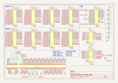
CE pins are common per Bank of four SRAMs so four tracks driving them. I already had CE tracks routed to meet those pin groups in last update as seen in FIC 486-GAC-2 cache coast VIP 95%.png blue text under under_U1_2 under_U1_3 😀 just needed confirmation.
majestyk wrote on 2024-02-10, 08:06:I also found that the system is unable to share the 8 TAG-bits for TAG and dirty/alt.
BIOS has an entry where you can select "combine alter and TAG bits" to enable/disable, but the result is the same - CTCM reports "Dirty TAG L2 -> n/a" and the memory performance is the same for "if dirty" and "if clean".
would be cool to locate 'alter' input of VT82C486A
majestyk wrote on 2024-02-09, 19:44:- U1 18 to M1 10 or M5 10? -> This seems like N/C, I can neither find a connection to any of the chips nor to the edge connector. And this makes sense, since pin 18 is I0-output, while the (grounded) pin 2 is I0-input. Buffer 0 is unused.
yep
majestyk wrote on 2024-02-09, 19:44:-cache slot a56 to M8 20? -> M8 pin 10 (A0)
-cache slot a57 to M4 20? -> M4 pin 10 (A0)
cool, this is Bank0_A0 and Bank1_A0
Progress report before your last post confirming CE pins was
"ERC 2 errors 0 warnings, DRC 0 errors 4 warnings"
After finalizing CE:
"ERC 0 errors 0 warnings, DRC 0 errors 1 warning"
One last unknown was A7 going from a18 to U1 pin 15 but also between pins 13 and 14. I looked at it harder and it finally hit me, its going around to avoid having to skip over A17_SR with a via under U1.
"ERC 0 errors 0 warnings, DRC 0 errors 0 warning"
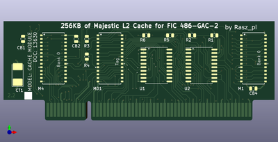
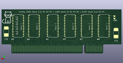
We are all green across the board! Footprints should be correct now, but better to print on paper, cut out and try if it lines up in the slot 😀 Its not 100% 1:1, I think original uses slim SOJ footprint, plus I made module slightly taller and fixing it now for 2 mm of difference would be a ton of work. Still needs some silkscreen work. Im still not 100% sure 64K R2 R4 configuration is a real thing 😀 needs testing. No chamfering a that requires Enig. Jlc does weakass goldplating and its stupid expensive + requires 5cmx5cm minimum board size (probably for holding boards while routing, we are smaller on one size) https://jlcpcb.com/quote/pcbOrderFaq/Gold%20Fingers
RockstarRunner you will have to use a nail file to slightly cut edges of the connector. Should be $7 + shipping for 5 boards
9 brand new SRAMs $13 https://www.digikey.com/en/products/detail/is … L-12JLI/1555403
2x 74F244 $2
3x 10uf $1 https://www.digikey.com/en/products/detail/ta … 106MLHT/6563099
4x 1uf $1 https://www.digikey.com/en/products/detail/ta … 05KGHTR/6563151
$24 total. Sadly those parts arent on the JLCPCB Basic List, nor even in stock as extended at the moment, maybe you can mail them and ask what it takes to pre-order - JLC assembly would be even cheaper than buying components from digikey. I know you offered to send me one, but I really dont need it. Ill gladly take some junk instead 😀 ISA MFM HDD controller or few 5.25 floppy disks, we can talk if the module works 😀
Other than that it was a fun ride, hope it works, needs some eyes on it checking for silly mistakes.
PS: found two other boards reusing VLB slot for proprietary cache, both totally different Re: Cache and video memory upgrade questions - HP Vectra VE 4/66
Well done, rasz, seriously! 😎
So, next step is putting together a prototype, I'll get on that tomorrow.
RockstarRunner wrote on 2024-02-10, 21:51:Well done, rasz, seriously! 😎
So, next step is putting together a prototype, I'll get on that tomorrow.
Next step is you or majestyk printing sram.kicad_pcb on paper in 1:1 scale, cutting it out with scissors and checking slot fitment and pin alignment (both slot and chip footprints). Would be good if you went over pcb comparing it to your photoshop traces one track at a time looking for mistakes, and going one more time over motherboard cache slot with a multimeter confirming ground/power pins just in case. Re-checking is quicker and cheaper than multiple board re-spins, its only $7 if you do it right on the first try 😀, little mistakes add up quickly.
Ill also go over the tracks one more time to space it all out better and slap some silkscreen. Final result:
Link to github repo https://github.com/raszpl/FIC-486-GAC-2-Cache-Module
First step of prototype was going to be paper version, like you said 👍
I live in Europe, so nothing about getting parts and pcb's will be cheap, and shipping costs + taxes etc.
Anyway; I have the chips, buffers and caps ordered, and I'll get the pcb design printed on paper when I visit my friend this evening, so I should have an idea if it fits by the end of the day.
I never thought this would ever become "WIP", but now we are nearly reaching finished product status.
Are the landings for the SRAM chips for SOP or SOJ chips only, or both?
RockstarRunner wrote on 2024-02-11, 07:15:I live in Europe, so nothing about getting parts and pcb's will be cheap, and shipping costs + taxes etc.
For reference standard 2 week shipping from jlcpcb to Poland is ~$8 and customs doesnt bother with any tariffs/taxes. Ebay sellers manage to ship stuff under $1, now that is a miracle of modern post subsidizing, developing country status my ass 😀
majestyk wrote on 2024-02-11, 08:10:I never thought this would ever become "WIP", but now we are nearly reaching finished product status.
To be fair like I said at the beginning it was just a puzzle. I replaced my daily ~hour of gaming (Into the Breach/FTL) with figuring out where hidden tracks would go 😀, looking at the log I spend ~6 hours at 100% attention on this project so far, all very fun. On the other hand designing something creative from scratch would feel like real job and I wouldnt be this enthusiastic without extra incentives 😀
majestyk wrote on 2024-02-11, 08:10:Are the landings for the SRAM chips for SOP or SOJ chips only, or both?
I used SOJ-28 footprint, minimally wider than SOJ-28L specified by original UM61256. From what Iv seen on digikey most if not all currently available 5V parallel SRAMs ship in this form factor. SOP-28 should also fit, maybe requiring to slightly bent legs inward.
I decide to actually read https://dosdays.co.uk/media/via/VIA_82C496G.pdf Despite being for never chipset it does look very familiar.
Page 9:
>Index (Tag/Cache Addr)
>64KB 8K x 8 x 2 A15:4#
>128KB 32K x 8 A16:4*
>256KB 32K x 8 x 2 A17:4#
>* A3SEL1 and A3SEL0 from the VT82C496G are connected to the other address bits of the data
cache
># CCS#0 and CCS# 1 are connected to the chip select of the two banks of data cache, respectively.
Furthermore, A3SEL0 and A3SEL1 are connected to one of the address lines (A3) of each bank,
respectively
Looks like I was correct deducing dual bank 64KB cache support. GAC-2 might even also support single bank 32KB 😮
VT82C496G does support 7+1 mode
>RX50h: Cache access mode
>− bit 4: combined alter bit for the write-back cache (don't care for write through)
maybe this could be modded into FIC bios if support was there in VT82C486A and registers are close enough.
New advances in technology now allow wafer thin prototype cache modules 😉
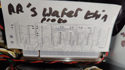
Scale was checked using a SOJ20 chip that although has less legs, has same pitch as the correct SRAM chips, and it lined up perfectly.
Looks ok to me
rasz_pl wrote on 2024-02-11, 08:41:I decide to actually read https://dosdays.co.uk/media/via/VIA_82C496G.pdf Despite being for never chipset it does look very fam […]
I decide to actually read https://dosdays.co.uk/media/via/VIA_82C496G.pdf Despite being for never chipset it does look very familiar.
Page 9:
>Index (Tag/Cache Addr)
>64KB 8K x 8 x 2 A15:4#
>128KB 32K x 8 A16:4*
>256KB 32K x 8 x 2 A17:4#
>* A3SEL1 and A3SEL0 from the VT82C496G are connected to the other address bits of the data
cache
># CCS#0 and CCS# 1 are connected to the chip select of the two banks of data cache, respectively.
Furthermore, A3SEL0 and A3SEL1 are connected to one of the address lines (A3) of each bank,
respectivelyLooks like I was correct deducing dual bank 64KB cache support. GAC-2 might even also support single bank 32KB 😮
VT82C496G does support 7+1 mode
>RX50h: Cache access mode
>− bit 4: combined alter bit for the write-back cache (don't care for write through)
maybe this could be modded into FIC bios if support was there in VT82C486A and registers are close enough.
The 3276gn1 BIOS is for 486 GIO VT, 486, 486 GAC-V , 486 GAC-2, 486 VIP IO, 486 GIO VP and 486 GVT2 - all (most?) of them have the VT82C486A chip. This BIOS has options for L1 WB, L2 WB/WT and L2 alter TAG 7+1 operation, so I guess in general the chipset supports it and the registers are being set correctly.
Question is why this fails on the GAC-2? I´ll have to try some of the other mainboards to find out if they are also affected.
P.S.- I still don´t understand the "4-contact thing". I mean, the 4 pins are shorted at the mainboard socket and they are shorted on the cache stick right at the goldfingers.
The only purpose I can imagine would be to reduce resistance, but there´s already a 22R resistor in the CE line, so this will improve nothing.
does it fit fine in the slot? all the way in?
Please do your photoshop magic once again and check if I didnt do any obvious stupid mistakes 😀
gerbers https://github.com/raszpl/FIC-486-GAC-2-Cache … e%20gerbers.zip
When ordering upload gerber and select "Remove Order Number: Specify a location", this will order 5 copies for $7 + shipping around $2-8 for standard land two week fare.
Fits in the slot fine
majestyk wrote on 2024-02-11, 19:38:The 3276gn1 BIOS is for 486 GIO VT, 486, 486 GAC-V , 486 GAC-2, 486 VIP IO, 486 GIO VP and 486 GVT2 - all (most?) of them have the VT82C486A chip. This BIOS has options for L1 WB, L2 WB/WT and L2 alter TAG 7+1 operation, so I guess in general the chipset supports it and the registers are being set correctly.
Question is why this fails on the GAC-2? I´ll have to try some of the other mainboards to find out if they are also affected.
Im looking at the BIOS 3276gn1, so far found spot where it turns off L2 at F000:9728 Here is where the magic happens:
_F000:9D9D loc_F9D9D: ; CODE XREF: sub_F9C30+157j_F000:9D9D ; sub_F9C30+162j_F000:9D9D mov cl, 50h ; 'P'_F000:9D9F call read_cl_from_VIA_F000:9DA2 and al, 0EFh_F000:9DA4 call write_cl_to_VIA_al_F000:9DA7 jmp short loc_F9DB3_F000:9DA9 ; ---------------------------------------------------------------------------_F000:9DA9_F000:9DA9 loc_F9DA9: ; CODE XREF: sub_F9C30+FAj_F000:9DA9 ; sub_F9C30+14Cj ..._F000:9DA9 mov cl, 50h ; 'P'_F000:9DAB call read_cl_from_VIA_F000:9DAE or al, 10h_F000:9DB0 call write_cl_to_VIA_al
first one clears bit 4 (write-back, combined tag/alter bit (default)), second one turns it on (write-back, no alter bit). Now to find where its called .. its called just above.
_F000:9D7E cmp edi, 2000000h_F000:9D85 ja short TAG_mode_8_F000:9D87 jmp short TAG_mode_7_1_F000:9D89 ; --------------------------_F000:9D89_F000:9D89 loc_F9D89: ; CODE XREF: sub_F9C30+146j_F000:9D89 cmp edi, 4000000h_F000:9D90 ja short TAG_mode_8_F000:9D92 jmp short TAG_mode_7_1_F000:9D94 ; ------------------------_F000:9D94_F000:9D94 loc_F9D94: ; CODE XREF: sub_F9C30+14Aj_F000:9D94 cmp edi, 8000000h_F000:9D9B ja short TAG_mode_8
There is code checking memory size, or maybe checking how much of ram is able to be cached, it automagically disables 7+1 mode if there is not enough cache for the ram installed. Do you have >32MB? 256KB is enough for 64MB TAG8 or 32MB TAG7+1.
majestyk wrote on 2024-02-11, 19:38:P.S.- I still don´t understand the "4-contact thing". I mean, the 4 pins are shorted at the mainboard socket and they are shorted on the cache stick right at the goldfingers. The only purpose I can imagine would be to reduce resistance, but there´s already a 22R resistor in the CE line, so this will improve nothing.
Person designing Cache socket pinout in the first place made a provision for driving all SRAM CE and WE pins individually, just in case I guess. In theory it would allow for some weird access patterns. Im sure it made some sense at the time. I wonder if a3 a2 or a23 are connected to anything on the motherboard side. Maybe it would be possible to make 512-1024KB cache 😀
rasz_pl wrote on 2024-02-11, 21:10:There is code checking memory size, or maybe checking how much of ram is able to be cached, it automagically disables 7+1 mode if there is not enough cache for the ram installed. Do you have >32MB? 256KB is enough for 64MB TAG8 or 32MB TAG7+1.
Shame on me, I did the tests with 48MB RAM forgetting (again) that the cacheable area is halved as soon as you snatch away 1 bit of the TAG bus. With 32MB it´s all perfect.
rasz_pl wrote on 2024-02-11, 21:10:Person designing Cache socket pinout in the first place made a provision for driving all SRAM CE and WE pins individually, just in case I guess. In theory it would allow for some weird access patterns. Im sure it made some sense at the time. I wonder if a3 a2 or a23 are connected to anything on the motherboard side. Maybe it would be possible to make 512-1024KB cache 😀
This might well be the case.
Sadly a2, a3 and a23 are N/C on the mobo...
majestyk wrote on 2024-02-12, 07:14:Shame on me
Gave me an excuse to exercise disassembly skills 😀 Two years ago it would have taken me hours, but now I was already reading this code after ~10 minutes.
majestyk wrote on 2024-02-12, 07:14:With 32MB it´s all perfect.
what big of a difference does it make in cachechk? Have you considered experimenting with jumpers on cache module to mod it down to 128/64KB?
majestyk wrote on 2024-02-12, 07:14:Sadly a2, a3 and a23 are N/C on the mobo...
There is still sliver of a chance FIC chose to never offer 512-1024 modules but chipset support is still there.
EDIT: Got an epiphany while sitting on the throne :] Above code from Bios 3276gn1 already checks for 32/64/128GB when disabling Alter bit, this only makes sense if you support 1MB L2. Means its either universal code module common for all VIA chipsets at the time (like VIA_82C496G), or VT82C486A supported 1M L2 from the start.
Hmmm, this would require wiring A18 A19 straight from chipset/VLB slot to cache module, and different module of course, too much work for small gain 😀.
Btw Alter bit is only supported by stealing TAG bit, no separate Alter input in the chipset 🙁
"Hmmm, this would require wiring A18 A19 straight from chipset/VLB slot to cache module, and different module of course, too much work for small gain"
This is great discussion though, while waiting for parts to build the prototype, but bit over my head.
Your epiphany might be true (despite the place where it occured).
The FIC 486-VIP-IO also has the VT82C486A (and runs the same BIOS) and it provides 9 x DIL32 sockets for 512K / 1MB cache.
And the (not very common) FIC PAK-3 has the same "VLB" cache slot and will profit from the GAC-2 cache module.
What´s wrong with this FIC 486 PAK-3 ??
I still have to dig it out in the attic and test it.
majestyk wrote on 2024-02-12, 13:38:Your epiphany might be true (despite the place where it occured).
The FIC 486-VIP-IO also has the VT82C486A (and runs the same BIOS) and it provides 9 x DIL32 sockets for 512K / 1MB cache.
FIC_486-VIP-IO_ESCOM.jpg
I totally missed that one, I was searching theretroweb for all boards listed under "VIA VT82C486 (GMC) [VIA VT82C482, VIA VT82C486A]" instead of going deeper into VT82C486A
majestyk wrote on 2024-02-12, 13:38:And the (not very common) FIC PAK-3 has the same "VLB" cache slot and will profit from the GAC-2 cache module.
What´s wrong with this FIC 486 PAK-3 ??
I didnt read that thread originally. Too bad it wasnt linked here earlier, I would have banged out nice looking VRM PCB to fit on same JLC order with cache slot 🙁
Did you solve 'some CPUs are slow' problem? Maybe its something in the bios. Norton 12 something result looks suspiciously like board constantly flushing CPU L1 cache.
>Today I ran some tests with a 486 DX2 66 (955) with write back cache on the FIC 486-PAK3. It´s detected by the BIOS correctly as DX2-66(WB) and all benchmarks are as they are supposed to be for a DX2-66.
>Maybe the regular DX2-66 were not offered by NCR and they just didn´t include them in their BIOS?
Hmm, would Bios hardcoded to treat all DXs as WB spam Flush pin frequently? That would still not explain score of 12. 12 is in hundreds of KHz cache flush spam territory - "Turbo in a retro PC - explanation and repair." - Necroware https://www.youtube.com/watch?v=i9DTA81xUN0
I somehow blanked out that this FIC was sold inside AT&T systems, and it seems to be a lot of models:
AT&T, INC. GLOBALYST 510/515
AT&T´s Globalyst 520 FIC PAK-3
NCR 3231
NCR 3232
NCR 3228-II
This project might turn out to be useful to more than one person after all 😀
I didnt see "AT&T Globalyst 515 restoration - from boring office box to retro 486 gaming PC"- Necroware https://www.youtube.com/watch?v=ZUt-3Y3vMso before either. Looking at the comments
1 "Necroware did I get that right: you found a module that would be electricaly compatible to your board, but mechanically too high to fit under the floppy drive"
erm, I made the reproduction slightly taller 😮 RockstarRunner did you check if paper cutout fits under the floppy? 😁
2 RetroSpector78 also got Globalyst 575 system, its another similar but not exact same board with VLB cache slot https://stason.org/TULARC/pc/motherboards/A/A … BALYST-550.html
3 RockstarRunner if the module works you will be able to sell of at least one pcb to Necroware 😀 Im sure he would love to solder it on video.
