Reply 100 of 119, by RockstarRunner
Rank
Member
@rasz_pl if you feel there is nothing else to tweak/test, I could order another set of boards, and confirm the revision is working.
@rasz_pl if you feel there is nothing else to tweak/test, I could order another set of boards, and confirm the revision is working.
There is no way of telling chipset you have only one bank, so with jumpers set to 128KB there are still CE/OE/WE signals being send to the other bank. I need to sit down and think about this some more 😀 are outputs from both clashing? is the dangling one still being activated? this would explain 128KB configuration crashing at the moment BIOS was initializing cache. 64KB one is weird, at first glance should 'just work'. This made me question my understanding of cache handling, I thought two banks would need some special mode where banks are interleaved, but there is nothing about it in the chipset datasheet.
I have pcb version with fixed footprints ready, but not yet uploaded. Should have some time during the weekend. Give me few days.
majestyk wrote on 2024-03-06, 19:08:The populated chips must match the jumpering, just like when the chips, buffers and jumpers are on the mainboard.
Hmm, when configured for 64KB Bios detects 64 because ?we are limiting TAG to 64? but SRAMs are still connected to A16 A17 so addresses dont wrap around? BIOS cache detection routine was fooled into thinking its working fine because .... hmm, damn I have to look at the code to understand it 😐
Edit: ... one hour later...
found it!
Edit: ... few hours later...
ok, I think I got it somewhat:
Edit: read it couple of days later and below code became much clearer, explanation updated 😀
Below is BIOS Post Code C1:
_F000:94C2 mov cl, 51h_F000:94C4 mov al, 0FEh_F000:94C6 mov sp, 94CCh_F000:94C9 jmp write_al_to_VIA_cl
FEh sets cache for 2 bank access 1MB.
_F000:94C9 ; ---------------------------------------------------------------------------_F000:94CC dw 94CEh_F000:94CE ; ---------------------------------------------------------------------------_F000:94CE mov al, 50h_F000:94D0 out 0A8h, al_F000:94D2 out 0E1h, ax_F000:94D4 mov al, 38h_F000:94D6 out 0A9h, al
38h sets "direct data SRAM access", I think this disables RAM completely. Afaik this is called CacheAsRam mode.
_F000:94D8 out 0E1h, ax_F000:94DA xor dx, dx_F000:94DC mov es, dx_F000:94DE assume es:nothing_F000:94DE mov ds, dx_F000:94E0 mov eax, 33CC33CCh_F000:94E6 mov ebx, 55AA55AAh_F000:94EC mov ds:dword_0, ebx_F000:94F1 mov ds:dword_8, eax_F000:94F5 cmp ds:dword_0, ebx_F000:94FA jnz loc_F9548
This is testing how much SRAM is mapped.
Its trying to write to higher and higher addresses and testing if original 0:0 value gets overwritten by wraparound
First testing if we can read from 0:0 what we just wrote there, this will indicate some L2 presence. Fails with DX=0
_F000:94FE cmp ds:dword_8, eax_F000:9503 jnz short loc_F9548
Offset 8 would map to Bank1 and we enabled both banks, we should fail here with only one bank installed with DX=0
_F000:9505 mov eax, 33CC33CCh_F000:950B mov ds:dword_8000, eax_F000:950F cmp ds:dword_0, ebx_F000:9514 mov dx, 800h_F000:9517 jnz short loc_F9548
Wrote to 8000h = 32KB, we are testing offset 0:0 for overwrites, failing here would mean wrap around = only 32KB L2 installed DX=800h
_F000:9519 mov dx, ds_F000:951B add dh, 10h_F000:951E mov ds, dx_F000:9520 assume ds:nothing_F000:9520 mov ds:0, eax_F000:9524 cmp es:dword_0, ebx_F000:952A mov dx, 1000h_F000:952D jnz short loc_F9548
Wrote to 1000:0000 (real mode) = 10000h = 64KB offset
ES was set to zero so we are again testing 0:0 for overwrite, failing here would mean wrap around = only 64KB L2 installed DX=1000h
_F000:952F mov dx, ds_F000:9531 add dh, 10h_F000:9534 mov ds, dx_F000:9536 assume ds:nothing_F000:9536 mov ds:0, eax_F000:953A cmp es:dword_0, ebx_F000:9540 mov dx, 2000h_F000:9543 jnz short cache_128kb
writing to 2:0 = 128KB offset
testing 0:0 for overwrite, failing here would mean wrap around = 128KB L2 installed DX=2000h
_F000:9545 mov dx, 4000h
4000h because its not testing anything beyond 128KB for wraparound, just assumes its gonna be 256KB at this point
_F000:9548 cache_128kb:_F000:9548 or dx, dx_F000:954A jz short disable_cache_F000:954C cmp dx, 800h_F000:9550 jz short one_bank_F000:9552 cmp dx, 2000h_F000:9556 jnz short two_banks
Already compared against 0 and 800h, passing here means DX is 2000h = 128KB 1 bank mode, jumping will bypass function switching from 2Bank to 1Bank config
_F000:9558 one_bank:_F000:9558 mov al, 51h_F000:955A out 0A8h, al_F000:955C out 0E1h, ax_F000:955E mov al, 0F6h_F000:9560 out 0A9h, al_F000:9562 out 0E1h, ax
Writing F6h into RX51 register sets 1MB 1 bank mode, we land here only with DX = 800h and 2000h so 32KB and 128KB configs.
_F000:9564 two_banks:_F000:9564 mov ax, dx_F000:9566 mov bl, ah_F000:9568 shr bl, 3
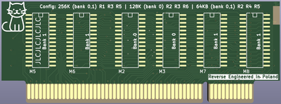
bl = 1 for 32KB, 2 for 64KB, 4 for 128KB and 8 for 256KB
_F000:956B cld_F000:956C xor ax, ax_F000:956E mov es, ax_F000:9570 mov eax, 55AA33CCh
We already determined capacity at this point and set appropriate number of banks active. Below is the actual L2 cache test to verify its all there. This test is performed using slowest 3-2-2-2 cache timings.
_F000:9576 sram_test:_F000:9576 mov cx, 2000h_F000:9579 xor di, di_F000:957B rep stosd_F000:957E mov cx, 2000h_F000:9581 xor di, di_F000:9583 repe scasd
SRAM testing, 'repe scasb' is ES:DI memory scan. Fill with marker, then scan verifying marker is there. 32KB at a time.
_F000:9586 jnz short bad_cache_F000:9588 mov cx, es_F000:958A add cx, 800h_F000:958E mov es, cx
Add 800h to es, effectively adding 32KB offset on every iteration
_F000:9590 not eax
Switching test pattern around every 32KB, not very robust but better than nothing.
_F000:9593 dec bl
bl keeps number of 32KB iterations
_F000:9595 jnz short sram_test_F000:9597 jmp short disable_cache_F000:9599 ; ---------------------------------------------------------------------------_F000:9599 bad_cache:_F000:9599 xor dx, dx
Successful sram_test would leave us with size encoded in DX, any fails will land above and zero it.
_F000:959B disable_cache:_F000:959B mov cl, 50h_F000:959D xor al, al_F000:959F mov sp, 95A5h_F000:95A2 jmp write_al_to_VIA_cl_F000:95A7 mov cl, 10h_F000:95A9 mov sp, 95AFh_F000:95AC jmp read_cl_from_VIA
RX10h is a VIA register responsible for ISA/DMA clock dividers, no detailed description, what is it doing in middle of cache check?
_F000:95B1 test al, 1_F000:95B3 mov si, 927Dh_F000:95B6 mov di, 9291h_F000:95B9 jnz short loc_F95C1_F000:95BB mov si, 9269h_F000:95BE mov di, 927Dh
Ram is disabled and there is no shadow mapping enabled, We are loading si with a const from EPROM. We use first bit of VIA register RX10h to decide which of two tables to pick from. No detailed RX10h documentation, just a hint about clock dividers.
_F000:95C1_F000:95C1 loc_F95C1:_F000:95C1 cmp dx, cs:[si]_F000:95C4 jz short loc_F95D0_F000:95C6 add si, 4_F000:95C9 cmp si, di_F000:95CB jb short loc_F95C1_F000:95CD jmp short loc_F95EC
Scanning for config matching DX
_F000:269 dw 0_F000:926B dw 0 ; no cache = disable everything_F000:926D dw 800h_F000:926F dw 1001h ; 32KB 1 bank, 7+1, cache line size: 4 bytes_F000:9271 dw 1000h_F000:9273 dw 140Ah ; 64KB 2 banks, 7+1, cache line size: 8 bytes_F000:9275 dw 2000h_F000:9277 dw 1803h ; 128KB 1 bank, 7+1, cache line size: 16 bytes_F000:9279 dw 4000h_F000:927B dw 140Ch ; 256KB 2 banks, 7+1, cache line size: 8 bytes. Why 8 and previous 16???_F000:927D dw 0_F000:927F dw 0 ; no cache = disable everything_F000:9281 dw 800h_F000:9283 dw 18F1h ; as above but slowest settings and cache line size: 16 bytes?_F000:9285 dw 1000h_F000:9287 dw 18FAh ; as above but slowest settings and cache line size: 16 bytes?_F000:9289 dw 2000h_F000:928B dw 18F3h ; as above but slowest settings and cache line size: 16 bytes?_F000:928D dw 4000h_F000:928F dw 18FCh ; as above but slowest settings and cache line size: 16 bytes?
Two sets of configs depending on DX being 0 800 1000 2000 4000.
Second set sets slowest SRAM timings and cache line size: 16 bytes for some reason.
_F000:95D0 loc_F95D0:_F000:95D0 mov cl, 51h_F000:95D2 mov al, cs:[si+2]_F000:95D6 mov sp, 95DCh_F000:95D9 jmp write_al_to_VIA_cl
setting size here
_F000:95DE mov cl, 50h_F000:95E0 mov al, cs:[si+3]_F000:95E4 mov sp, 95EAh_F000:95E7 jmp write_al_to_VIA_cl
and cache mode here
_F000:95EC loc_F95EC:_F000:95EC shr edx, 10h
DX is one of 0 800 1000 2000 4000. shr edx, 10h doesnt make sense here? result always 0?
_F000:95F0 mov ax, dx_F000:95F2 mov cl, 5Eh_F000:95F4 mov sp, 95FAh_F000:95F7 jmp write_al_to_VIA_cl
What is happening here? is it working at all? This might be landing on bit 6 L2 WB/WT?
RX5Eh: misc. cache control
− bit 7: CPU internal cache 0: write-through 1: write-back
− bit 6: external cache 0: write-back 1: write-through
− bit 5: pin 72 usage 0: BLAST# 1: CACHE# (P24T)
− bit 4-0: other usage
_F000:95FC mov cl, 42h_F000:95FE xor al, al_F000:9600 mov sp, 9606h_F000:9603 jmp write_al_to_VIA_cl
disabling some non cacheable area
_F000:9608 mov al, 0_F000:960A mov sp, 9610h_F000:960D jmp CMOS_L1cache_OnOff
Disabling/enabling L1 cache according to CMOS stored value
_F000:9612 shr esi, 10h_F000:9616 mov sp, si_F000:9618 clc_F000:9619 retn
well that was unproductive 😀 I still dont know whats going on and why BIOS gets fooled by 256KB of cache with TAG ram limited to 64KB.
The only knowledge gained is definite no on 512KB and 1MB cache support with this bios without modding.
EDIT: L2 SRAM test is very rudimentary:
First stage checks on 32KB 64KB 128KB boundaries for wraparound.
Second stage actually validates full capacity using one constant per 32KB segment.
Our 256_as_64 module will not wrap around on its own, the only difference is TAG limited to 16K addresses. Why is TAG making a difference here? Is TAG still somehow used in "direct data SRAM access"/CacheAsRam mode??
Ignoring TAG our module should not have stopped at 64KB detection, so TAG must still play a role.
Btw this is not the end of Cache checking. After completing C1 bios executes this just to be sure:
_F000:073E mov ax, 0_F000:0741 mov ds, ax_F000:0743 mov bx, ds:word_472_F000:0747 xor di, di_F000:0749 mov es, di_F000:074B mov cx, 4000h_F000:074E mov eax, 3C3CC3C3h_F000:0754 rep stosd_F000:0757 mov cx, 4000h_F000:075A xor di, di_F000:075C repe scasd_F000:075F jnz error_beep ; continous beeeping_F000:0763 mov ds:word_472, bx_F000:0767 mov al, 0C5h_F000:0769 mov dx, 80h_F000:076C out dx, al_F000:076D mov sp, 773h_F000:0770 jmp bios_shadowOn
additional 64KB test with enabled L1 and L2 cache, if this fails board goes into constant Pc speaker Beep loop.
/end edit
Aaaanyway
To test 64KB I could have to make additional jumpers pulling all pins 1 and 26 to VCC, thats just too much work for a silly test.
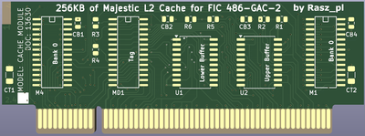
128KB mode didnt work with both banks populated because both Banks were being activated at the same time, R5 R6 doesnt deactivate Bank1, it just lets BANK0 take over one more address bit to make up for the missing bank at the cost of halving capacity. The only way of testing 128KB mode is to solder just 4 BANK0 SRAMs.
rasz_pl wrote on 2024-03-16, 23:21:The only knowledge gained is definite no on 512KB and 1MB cache support with this bios without modding.
The alternative BIOS for this FIC chipset platform "4.27GN2A" does support 512K and 1Mb cache, but it comes without video BIOS so an extra ISA graphics card would be necessary. This BIOS version also includes the "PCI module" for boards with the VIA 505 bridge chip like the 486 VIP-IO.
______________________________
I think with the 256K we´re at the point of bliss already.
A PCB-version with the Vcc/Vss issue resolved would be great. If some people really need 128K they can just populate 4 chips.
We printed the PCB, the SRAM pads look quite the same as the last one, you did link the latest version?
Bottom line is it can be soldered by someone who is good, but to make it possible for less capable people (myself 😉) the pads could be maybe twice as wide, to the outside direction.
picture? From the old one
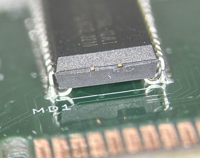
it looked like problem was on the inside with chip legs laying on base pcb, not the outside. The new one should be hot air solderable. Tin all pads with solder, put chip on top, 30 seconds with hot air and its done.
I slapped extra ridiculously oversized footprint into this:
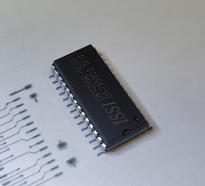
can you take a photo of this one? I dug around in my stash and I dont have any chips in this weird footprint 🙁 and cant find any 3D models to fit in kicad.
edit: updated Re: FIC 486-GAC-2 and proprietary cache module - Prototype works! Revision in progress. with better bios cache test description
By 'same as last one' I meant the version where you increased the pads going under the chip, to which we determined makes that much better for hot air soldering, but still difficult with an iron, hence why wider pads to the outside direction could help with that
I'll try and get that printed/checked when I get access to printer again. Thanks.
I think the pcb is not feeling well
EDIT: Oh snap, too clever for us. It's the oversized one just for the test.
After blood returned to brain from weight lifting, we understood the assignment 😆
Looks good to solder via hot air or iron, good stuff.
miisalo wrote on 2024-03-22, 18:11:EDIT: Oh snap, too clever for us. It's the oversized one just for the test.
Cmon, Im not that incompetent 😜
RockstarRunner wrote on 2024-03-22, 18:22:Looks good to solder via hot air or iron, good stuff.
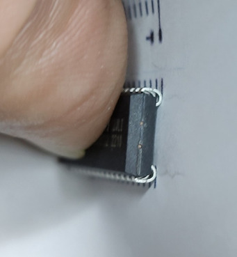
too bad you didnt line it up with second row so I could precisely see where metal touches. Inner size looks almost perfect, outer slightly too long?
rasz_pl wrote on 2024-03-22, 19:40:Cmon, Im not that incompetent 😜
too bad you didnt line it up with second row so I could precisely see where metal touches. Inner size looks almost perfect, outer slightly too long?
We lift iron, we no blood in brain, we stupid. Seriously after our regular gym session we even count one, two, many, lots..... *staring at distance* .
But I don't think out size is too long as long as those can be fit in to the module nicely. Probably easier to solder using normal solder and iron as you can warm up the pads with "regular" solder tip. Then again, are people who don't have good equipment and soldering skills going to solder these anyway.
fitting those longer pads wasnt a breeze, but its done
moved small caps closer to make them actually do something, hope vias in pads wont make too much trouble while assembling
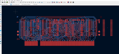
updated github, https://github.com/raszpl/FIC-486-GAC-2-Cache … ain/gerbers.zip looks fine in gerber viewer
Great work, this looks brilliant!
The "proprietary cache module" just became far less proprietary. I love this kind of stories with happy endings.
I'll order another run of 5 PCBs today.
Exciting stuff.
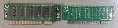
Pcbs turned up! We have edge connectors this time 😆
Will assemble this Friday, I expect, then I'll report the results.
Good to know...so I´ll wait another couple of days before I order some PCBs for myself.
Fingers crossed I didnt screw anything up while stretching those footprints 😀
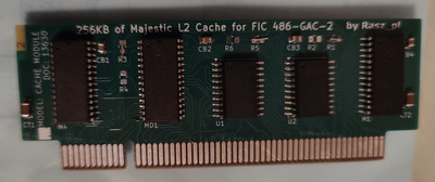
Miisalo transplanted the chips from the prototype to the final revision today!
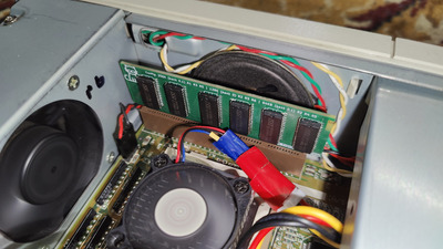
First test, the machine didn't boot, but turned out there was some solder balls hiding in a couple of spots, a side effect of resoldering chips and being bit tired from hard weight training.
After clean up though...
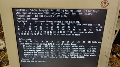
Final revision confirmed working!
Great work, we did it!!!
Note: I have parts for two modules, if someone needs, either assembled or kit form. P.M. for details.
👍
Ill update github repo tonight with pictures and success report.
I'm thinking, would the RetroWeb want links to the GitHub for the relevant boards pages?
