VOGONS


First post, by LChackr

User metadata
Rank Newbie
Rank
Newbie

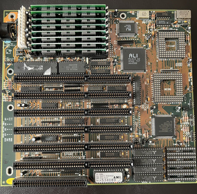
On this motherboard (pic attached) there is both a soldered 386DX and an open socket. What happens if I drop a CPU in the socket? Does it override the soldered one? I don't see a jumper that disables the CPU and I don't want to mess something up by populating the socket.

Also, it looks like this board is clocked at 40MHz. I have a 33MHz Cyrix 486DLC. Does anyone happen to know how well these chips tolerate overclocking? I do plan on adding a heatsink and fan because I know it already gets very warm just running at 33MHz.

Thanks!

Attachments

  • MB.jpeg
    Filename
    MB.jpeg
    File size
    1007.62 KiB
    Views
    1110 views
    File license
    CC-BY-4.0

Reply 1 of 18, by dominusprog

User metadata
Rank Member
Rank
Member

First of all clean the corrosion with white vinegar 😀

Second, read the manual and remember you have to change the crystal to 66.0MHz for your Cyrix 33MHz.

Manual
https://theretroweb.com/motherboards/s/abit-ab-fa3#downloads

Duke_2600.png
A-Trend ATC-1020 V1.1 ❇ Cyrix 6x86 150+ @ 120MHz ❇ 32MiB EDO RAM (8MiBx4) ❇ A-Trend S3 Trio64V2 2MiB
Aztech Pro16 II-3D PnP ❇ 8.4GiB Quantum Fireball ❇ Win95 OSR2 Plus!

Reply 2 of 18, by LChackr

User metadata
Rank Newbie
Rank
Newbie
dominusprog wrote on 2023-08-19, 19:32:

First of all clean the corrosion with white vinegar 😀

Yes. I took that picture between cutting off the battery and cleaning the corrosion. It's now nice and clean and looks like all the traces are intact. 😀

dominusprog wrote on 2023-08-19, 19:32:

Second, read the manual and remember you have to change the crystal to 66.0MHz for your Cyrix 33MHz.

Yes, I found that. (I love The Retro Web.) There is no jumper for CPU selection at all. Just cache. The layout doesn't exactly match ABit AB-FA3, and it's marked SER 386-AD3. It doesn't exactly match the board on that page either. Interestingly the Retro Web photo shows someone having added an i386DX-33 chip along side the soldered Am386DX-40.

https://theretroweb.com/motherboards/s/serite … -ser-386-ad-iii

If I could get away with pushing the Cx486DLC to 40MHz that would be great but I don't want to fry the chip. I know people have had mixed results and I would for sure be adding active cooling. I guess I should go oscillator shopping.

Reply 3 of 18, by H3nrik V!

User metadata
Rank Oldbie
Rank
Oldbie

What about those soldered jumpers, JP8 and JP9, sitting between the soldered CPU and what I guess is the cache tag chip, could they maybe be something? Wouldn't mess with it without confimation from a manual, though 🤣

Please use the "quote" option if asking questions to what I write - it will really up the chances of me noticing 😀

Reply 4 of 18, by H3nrik V!

User metadata
Rank Oldbie
Rank
Oldbie
H3nrik V! wrote on 2023-08-19, 20:16:

What about those soldered jumpers, JP8 and JP9, sitting between the soldered CPU and what I guess is the cache tag chip, could they maybe be something? Wouldn't mess with it without confimation from a manual, though 🤣

Oh, the manual clearly states about JP8 at least "factory setting do not alter".

Please use the "quote" option if asking questions to what I write - it will really up the chances of me noticing 😀

Reply 5 of 18, by LChackr

User metadata
Rank Newbie
Rank
Newbie
H3nrik V! wrote on 2023-08-19, 20:17:

Oh, the manual clearly states about JP8 at least "factory setting do not alter".

Haha, yes. I've looked over the board well and found all the JP headers. None of them are good candidates for me to touch. Interestingly neither of the candidate boards have jumpers for CPU selection, so I assume it does detect the inserted CPU and switches automatically? The one board that has a CPU jumper selects for the Cx486DLC vs the 386DX and I assume that has to do with the cache coherency lines and not which CPU to use.

Reply 7 of 18, by LChackr

User metadata
Rank Newbie
Rank
Newbie
DerBaum wrote on 2023-08-19, 21:18:

http://www.amoretro.de/2013/01/kmc-a419-8-ace … otherboard.html
This looks quite a lot like your board...

Nailed it! It looks like my board is a bit newer than the one in the pics. The date codes on chips point to manufacture sometime after week 41 1992, and my board (solder side) is marked week 48 1993.

Using the info on that page I found a discussion on Vogons from a few years ago about RAM and someone found that it matches this board:

https://theretroweb.com/motherboards/s/jamico … 0a-486dlc-386dx

It matches perfectly. From the manual it references that this is a 486DLC/386DX board. That leads me to suspect that the CPU socket is literally intended to be for a 486DLC? Considering that some of the boards we've been discussing have a jumper to set the DLC (cache lines?) that the socket is probably automatically set for DLC operation if populated. 🤔

Cx486DLCs are just rare and expensive enough that I don't want to risk dropping mine in if I don't know what will happen. 😀

Reply 8 of 18, by LChackr

User metadata
Rank Newbie
Rank
Newbie

PAGING RayeR! (I tagged you in the quote)

Vogons is such a great resource. I was poking around and found that RayeR has a similar board and modded his with a socket.

RayeR wrote on 2022-12-15, 10:05:

BTW I did the socket mod on this MB as mine has soldered Am386DX and I wanted also use PGA CPUs like my Tx486DLC that is supported in BIOS. I use FLT# pin of onboard CPU to disable it via jumper so I can switch back. I also populated 256kB cache, I had to jumper it by trial-error to be recognized by BIOS. Now I make it working with PATA SSD and installed Win95 there, it runs surprisingly well 😀
http://rayer.g6.cz/hardware/retropc2.htm

Your board looks like mine except mine already has a socket from the factory. FLT# (pin 54) on mine looks like it's not connected to anything. Does this suggest that the socket will be ignored? Would I need to do a mod like yours to have the option of trying another CPU? Would it hurt anything to try? I'm willing to try as long as it's not likely to damage my DLC chip. 😀

Reply 10 of 18, by rasz_pl

User metadata
Rank l33t
Rank
l33t

Sockets on most of those price optimized micro-AT 386 boards are not for upgrading or any user use. They were manufacturing universal boards to be able to use cheapest CPU possible every day/week. CPU (and cache) were the last components mounted on the board before shipping them out.
cant use the other spot without modding or removing cpu

H3nrik V! wrote on 2023-08-19, 20:17:
H3nrik V! wrote on 2023-08-19, 20:16:

What about those soldered jumpers, JP8 and JP9, sitting between the soldered CPU and what I guess is the cache tag chip, could they maybe be something? Wouldn't mess with it without confimation from a manual, though 🤣

Oh, the manual clearly states about JP8 at least "factory setting do not alter".

jp10 goes to E13, NC on 386, FLUSH# on 486DLC. JP11 is F13 , again not connected on 386, but A20M# on 486DLC. I cant see where JP9 is going but im guessing its also for 486DLC cache handling. Curiously https://theretroweb.com/motherboards/s/jamico … 0a-486dlc-386dx has two pictures, one with jumpers and soldered 386, other has just pcb links soldered shut but also 386 and no pga socket. I dont know intricacies of 486dlc cache pumper magic, you would have to dig into one of feipoa threads.

Last edited by rasz_pl on 2023-08-20, 01:15. Edited 1 time in total.

Open Source AT&T Globalyst/NCR/FIC 486-GAC-2 proprietary Cache Module reproduction

Reply 11 of 18, by DerBaum

User metadata
Rank Oldbie
Rank
Oldbie
LChackr wrote on 2023-08-19, 22:11:
PAGING RayeR! (I tagged you in the quote) […]
Show full quote

PAGING RayeR! (I tagged you in the quote)

Vogons is such a great resource. I was poking around and found that RayeR has a similar board and modded his with a socket.

RayeR wrote on 2022-12-15, 10:05:

BTW I did the socket mod on this MB as mine has soldered Am386DX and I wanted also use PGA CPUs like my Tx486DLC that is supported in BIOS. I use FLT# pin of onboard CPU to disable it via jumper so I can switch back. I also populated 256kB cache, I had to jumper it by trial-error to be recognized by BIOS. Now I make it working with PATA SSD and installed Win95 there, it runs surprisingly well 😀
http://rayer.g6.cz/hardware/retropc2.htm

Your board looks like mine except mine already has a socket from the factory. FLT# (pin 54) on mine looks like it's not connected to anything. Does this suggest that the socket will be ignored? Would I need to do a mod like yours to have the option of trying another CPU? Would it hurt anything to try? I'm willing to try as long as it's not likely to damage my DLC chip. 😀

On the unpopulated version the pin seems to be unconnected. So i would guess the RayeR modwire is necessary to make the sockeded CPU work...

FCKGW-RHQQ2

Reply 12 of 18, by LChackr

User metadata
Rank Newbie
Rank
Newbie
rasz_pl wrote on 2023-08-20, 00:56:

Sockets on most of those price optimized micro-AT 386 boards are not for upgrading or any user use. They were manufacturing universal boards to be able to use cheapest CPU possible every day/week. CPU (and cache) were the last components mounted on the board before shipping them out.
cant use the other spot without modding or removing cpu

Figures. The mod is easy enough.

H3nrik V! wrote on 2023-08-19, 20:17:

jp10 goes to E13, NC on 386, FLUSH# on 486DLC. JP11 is F13 , again not connected on 386, but A20M# on 486DLC. I cant see where JP9 is going but im guessing its also for 486DLC cache handling. Curiously https://theretroweb.com/motherboards/s/jamico … 0a-486dlc-386dx has two pictures, one with jumpers and soldered 386, other has just pcb links soldered shut but also 386 and no pga socket. I dont know intricacies of 486dlc cache pumper magic, you would have to dig into one of feipoa threads.

Hmm. It looks like JP9, JP10, and JP11 are soldered into the correct position for DLC operation on my board, yes? Since if it was a 386 they are NC by default so theoretically it wouldn't matter anyway ...

Reply 13 of 18, by Horun

User metadata
Rank l33t++
Rank
l33t++

Good looking 386 board. If it were mine would not mess with it if it runs perfect the way it is.. specially if it came with soldered jumpers (there is a reason ;p)

Hate posting a reply and then have to edit it because it made no sense 😁 First computer was an IBM 3270 workstation with CGA monitor. Stuff: https://archive.org/details/@horun

Reply 14 of 18, by Sphere478

User metadata
Rank l33t++
Rank
l33t++

It honestly blows my mind that they didn't run the flt pin to vcc through a 1k resistor and to a floating gnd assigned pin on the cpu socket. installing a cpu would gnd flt and disable the onboard cpu

They made these boards not upgradable to the laymen by not doing this.

Sphere's PCB projects.
-
Sphere’s socket 5/7 cpu collection.
-
SUCCESSFUL K6-2+ to K6-3+ Full Cache Enable Mod
-
Tyan S1564S to S1564D single to dual processor conversion (also s1563 and s1562)

Reply 15 of 18, by H3nrik V!

User metadata
Rank Oldbie
Rank
Oldbie
Sphere478 wrote on 2023-08-20, 04:32:

It honestly blows my mind that they didn't run the flt pin to vcc through a 1k resistor and to a floating gnd assigned pin on the cpu socket. installing a cpu would gnd flt and disable the onboard cpu

They made these boards not upgradable to the laymen by not doing this.

OTOH, how plausible would it be back in the day to upgrade past a 40MHz DX?

Please use the "quote" option if asking questions to what I write - it will really up the chances of me noticing 😀

Reply 16 of 18, by rasz_pl

User metadata
Rank l33t
Rank
l33t

I dont think anyone was thinking about mass retail upgrades market during 386 generation. Upgrades usually came in form of cards with cpu interposers or whole CPU modules (Evergreen, Kingston Now series etc) https://www.ardent-tool.com/CPU/386_upgrade.html and were neither all that common nor financially justified (usually you could do better selling whole computer and buying faster used one for same money).
I think this might have even happened by accident with 486 boards being build to accept multiple CPU configurations by default creating this expectation from the users of being able to just swap faster part later.
With 486 upgrade meant you could sell old CPU to recuperate some of the cost, with 386 no such luck. CPU was either soldered, or worthless as all 386 boards came with one.

H3nrik V! wrote on 2023-08-20, 04:37:

OTOH, how plausible would it be back in the day to upgrade past a 40MHz DX?

close to zero up to 1992 when Cyrix started releasing and licensing its SLC/DLC cores, then very slight 😀

Open Source AT&T Globalyst/NCR/FIC 486-GAC-2 proprietary Cache Module reproduction

Reply 17 of 18, by LChackr

User metadata
Rank Newbie
Rank
Newbie
Horun wrote on 2023-08-20, 04:01:

Good looking 386 board. If it were mine would not mess with it if it runs perfect the way it is.. specially if it came with soldered jumpers (there is a reason ;p)

Trust me, I know. The draw of this mod is that it's a single pin, and it's reversible. If it involved anything more complicated then I wouldn't even consider it. It's in an old AT case and since I don't need the keyboard lock I am considering using that lock switch activate/deactivate the mod. That seems really clean to me - I can switch between the CPUs with a quick flip of a switch and not even need to open the case. That idea is just so novel, and so attractive...

Reply 18 of 18, by Sphere478

User metadata
Rank l33t++
Rank
l33t++
H3nrik V! wrote on 2023-08-20, 04:37:
Sphere478 wrote on 2023-08-20, 04:32:

It honestly blows my mind that they didn't run the flt pin to vcc through a 1k resistor and to a floating gnd assigned pin on the cpu socket. installing a cpu would gnd flt and disable the onboard cpu

They made these boards not upgradable to the laymen by not doing this.

OTOH, how plausible would it be back in the day to upgrade past a 40MHz DX?

Cyrix had your back, there were also a few other neat interposer style dealieos also.

Sphere's PCB projects.
-
Sphere’s socket 5/7 cpu collection.
-
SUCCESSFUL K6-2+ to K6-3+ Full Cache Enable Mod
-
Tyan S1564S to S1564D single to dual processor conversion (also s1563 and s1562)