First post, by jakethompson1

- Rank
- Oldbie
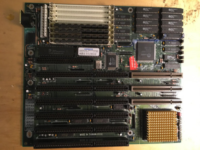
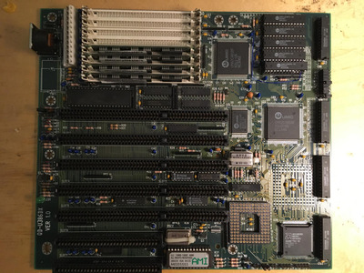
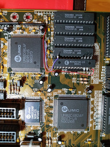
The UM481 and UM491 are two 386/486 combo chipsets that support write-back external cache up to 256KB.
They have an issue in that they support neither 7+1 tag mode to rob a bit of the Tag RAM for a dirty (alter) bit nor do they support switching the external cache from write-back to write-through mode to avoid the need for a dirty bit.
As a refresher, these chipsets (and most other 486 chipsets) read in cache lines of 16 bytes. If the CPU changes just a single bit in that entire cache line, then once it is time to bring in a different part of DRAM into that cache line, the entire 16 bytes must be written back to RAM first. Sometimes the board maker will omit that Dirty Bit from the design altogether, and instead wire the ALT pin of the chipset to a pull-up resistor and leave the ALTWE# pin floating. The chipset attempts to write the alter bit and it goes nowhere; when it tries to read the alter bit, it always reads a 1. So, if the CPU causes a cache line to be read into SRAM, then causes another one to be read without changing anything, the cache has to write out those 16 bytes anyway. It is not hard to see that this hurts performance.
Some boards at least leave a socket to add the Dirty RAM even if it is left out at the factory, but I wanted to try PC-Engineer's modification (suggested here: Re: 486 cache/ram speed issue with write-back) on two boards that did not. It was successful.
The UM82C481 has ALT on pin 37, ALTWR# on pin 38, and TRWR# on pin 39.
The UM82C491 has ALTWR# on pin 72, ALT on pin 73, and TRWR# on pin 74.
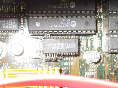
- Locate the Tag RAM by determining which of the nine SRAMs has the TAGWR# connected to WE# (pin 27) on the SRAM.
- Create a makeshift Dirty RAM. You take another 32kx8 SRAM and break off the data pins (11, 12, 13, 15, 16, 17, 18, 19) and WE# (27). Piggy back it on top of an intact SRAM and solder down the remaining pins on the top one. This combination is your new Tag RAM.
- There should be a pull-up resistor on your board nearby to the ALT pin; use a multimeter to make sure. Run a wire from any one of the 8 remnants of the data pins of your Dirty RAM to the side of that pull-up resistor that has continuity to the ALT pin.
- This is the hard part, run a wire from the ALTWR# pin to remnant of the WE# pin on your Dirty RAM.
I asked behind the scenes and got some good advice. Use 30 gauge wire (wire-wrap wire), a syringe of SMD291 flux, and 0.38 mm solder. Pre-tin the bare ends of your wire and make sure you solder to the top of the ALTWR# pin where it goes into the chip. You will be aligning the wire over top that pin and touching it with the tip of the iron for a split second. Don't try to solder to the pad or solder to the vertical portion of the wire. I attempted that on another board and am now having to clean it up as all the pins are now bridged together with solder and some got crossed onto the wrong pads altogether.
On the UM491, 486DX2-66, cachechk scores improved to 16 uS/KB, 24 uS/KB, and 36 uS/KB (36 down from 51).
On the UM481, 386DX-40, cachechk scores improved to 39 uS/KB and 60 uS/KB (60 down from 92). With the modification it is now on-par with my ALi M1429 which uses 7+1.
What cachechk scores do you get on your 386DX-40 and 486DX2-66 systems?
Who else has a write-back-only chipset with no 7+1 support? I believe there were some OPTi that fall into this category also.