First post, by JF_Sebastian

- Rank
- Newbie
Hello colleagues,
First of all, I would like to say that I have really tried to read up. But I am still confused.
Yesterday I got an offer for an "Asus P/I-P55T2P4 Rev 3.10" with SRAM chip socket and slot for a COAST module. I'm very interested in it, but I don't really understand the SRAM upgrade for more cache RAM in the manual.
My questions are:
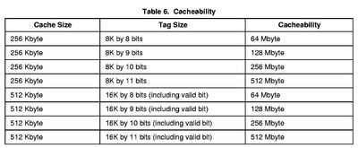
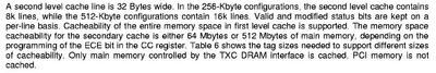
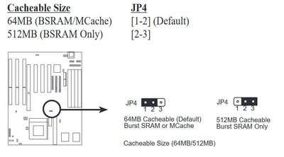
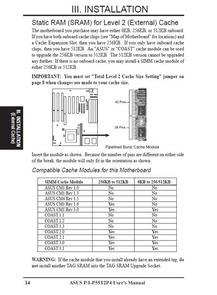
- Can I get more cacheable RAM with just an SRAM chip in the socket instead of a COAST module? I have read on the Internet about users who have upgraded to 96 MB of cacheable RAM with an SRAM chip. How does this work? The manual says that a cacheable area of more than 64MB is only possible with pipeline burst cache, but only the COAST module has this.
- What good is an SRAM chip if the cacheable area can only be extended with pipeline burst cache, which is only on the COAST modules?
- Do the SRAM chip and a COAST module have different purposes or tasks?
I would be very happy if someone could explain this to me for dummies?
Best regards and have a nice day!
JF
Boot Up or Shut Up!
________________________
Asus P/I-P55T2P4 Rev. 3.10
Asus USB/MIR Rev. 1.11
AMD-K6-III/450AFX @6x83MHz; 2.4V
4x128MB EDO RAM 60ns
MATROX Mystique MGA-1064SG-D 4MB
Diamond Monster 2 8MB
DELOCK 91620 - CF to IDE
________________________