VOGONS


First post, by 1200XL M.U.L.E.

User metadata
Rank Newbie
Rank
Newbie

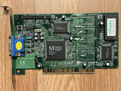
I recently bought a Am486DX4-100 system from eBay and am discovering it seemingly has some high quality components!

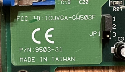
One of those components is a PCI video card with a S3 ViRGE/DX chip. The FCC ID is ICUVGA-GW503F. Google results say this card was made by Gainward. The company is still around today.

The VGA Musuem site has a picture of this card (but with more onboard memory) and identifies it as a Gainward CardExpert.

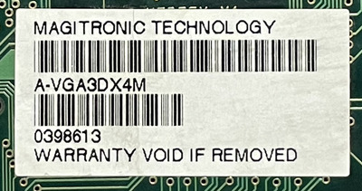
The back of the card has an identifying sticker that says this card has something to do with Magitronic Technology. I could not get any meaningful search results when looking them up.

I am looking for an owners manual for this card so I can better understand three features.

1) What does JP1 near the PCI edge connector control?
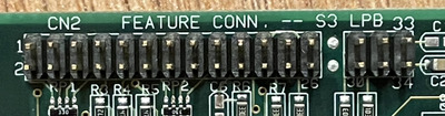
2) What is the purpose of the CN2 connector at the top of the card?
3) What is the purpose of the LPB connector at the top of the card?

Thanks!

Attachments

  • IMG_4913.jpg
    Filename
    IMG_4913.jpg
    File size
    402.16 KiB
    Views
    155 views
    File license
    Public domain
  • IMG_4912.jpg
    Filename
    IMG_4912.jpg
    File size
    536.73 KiB
    Views
    155 views
    File license
    Public domain
  • IMG_4911.jpg
    Filename
    IMG_4911.jpg
    File size
    442.74 KiB
    Views
    155 views
    File license
    Public domain
  • IMG_4910.jpg
    Filename
    IMG_4910.jpg
    File size
    1.73 MiB
    Views
    155 views
    File license
    Public domain

Reply 1 of 1, by Horun

User metadata
Rank l33t++
Rank
l33t++

Unfortunately the old Gainward aka Cardex archive does not have manuals. Yours would be the Genesis SV+ of which there were two variants, a 2Mb and 4MB.
http://web.archive.org/web/19980212173655/htt … tml/product.htm
CN2 is a (VESA/VGA) Feature Connector. Early VR headsets, MPEG2 Decoder cards, etc used it to have a direct connection to the video instead of going through the ISA, VLB or PCI bus to transport the data to the video card.
The S3 LPB connector part allows an external device to directly access/change the LPB registers in the S3 chip, a bit of info here on page 24-2:
http://www.bitsavers.org/components/s3/DB019- … tor_Aug1996.pdf
JP1 could be for memory type or something else, can you post a picture of the back of the card ? That is all I got 😀

Hate posting a reply and then have to edit it because it made no sense 😁 First computer was an IBM 3270 workstation with CGA monitor. Stuff: https://archive.org/details/@horun