VOGONS


First post, by ApostolCV

User metadata
Rank Newbie
Rank
Newbie

Hello there 😀
For some time now I have owned two strange Slot-kets.
When i get first and try to use it i came to the conclusion that it was broken. System with it do no POST .
But when i get second with same issue i try to find what can be wrong .
So i take multimiter and some old documentation with SLOT 1 and Socket 370 pinout.
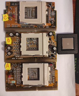
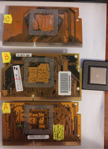
Downwards you can see photo with 3-x Slot-kets : were market by me like A,B,C.
Slot-kets B,C do not work/post . Slot-ket A is full-workerd with Support PPGA 370 CPU (Mendocino) , Coppermine (P3/Celeron), VIA CPUs.
[attachment=-1]frontS1.jpg[/attachment]

back.jpg
Filename
back.jpg
File size
484.26 KiB
Views
560 views
File license
GPL-2.0-or-later

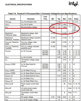
With some measurement i discovered that at slotkets "B,C" voltage at socket pin AN11 that should be VTT 1.5V is 2.0V.
On slotket "A" that work it's correct and equal 1.5V.
I chech mottherboard ...
In both cases, the motherboard outputs 1.5V on pin A1 of the Slot 1 connector. A1 is VTT voltage.
Does anyone have any thoughts about this? Or have you encountered something similar?

Attachments

Reply 1 of 8, by H3nrik V!

User metadata
Rank Oldbie
Rank
Oldbie

Have you tried measuring with a multimeter if there's connection between the pin on the socket and the pin on the slot? Maybe in some older spec, VTT should be ~2V and is then made from the VCore? Did you measure the voltage with a CPU inserted?

Please use the "quote" option if asking questions to what I write - it will really up the chances of me noticing 😀

Reply 2 of 8, by ApostolCV

User metadata
Rank Newbie
Rank
Newbie
H3nrik V! wrote on 2024-01-10, 22:01:

Have you tried measuring with a multimeter if there's connection between the pin on the socket and the pin on the slot? Maybe in some older spec, VTT should be ~2V and is then made from the VCore? Did you measure the voltage with a CPU inserted?

Hello,H3nrik V!
First .I do measurment with powered on motherboard when SLOTKET in motherboard and CPU is in socket.
At all slotkets (A,B,C) VTT voltage from pin A1 PIN arrives at the pin AN11 passing through a resistor assembly 55 Ohm.
Sorry, i must to correct you but VTT voltage about 2V is not normal and is to high . I went to internet and found documentatin for pentium 2 .
Basic VTT is about 1.5V . Here is proof.

P2specs.jpg
Filename
P2specs.jpg
File size
73.67 KiB
Views
521 views
File license
GPL-2.0-or-later

Reply 3 of 8, by Grem Five

User metadata
Rank Member
Rank
Member

B and C are both PPGA Celeron only Slotkets and when I look up the data sheet those Celeron cpus it lists pin AN11 as: AN11 - Reserved for future use

So does it matter that they are at 2 volts? I dont know I'm asking...

Edit: BTW Slotket C appears to be a 'Matrix S370-Adaptor PPGA Celeron / 66, 100 / auto voltage' and Slotket B appears to be a 'Procomp D370A ver: 1.0 PPGA Celeron / 66, 100 / auto voltage'

Edit #2: I checked and I have a Slotket C (I was wondering why it looked familiar) it boots with a 400 MHz Mendocino Celeron and when its running if I check AN11 my multimeter reads 2.01 volts.

Reply 4 of 8, by H3nrik V!

User metadata
Rank Oldbie
Rank
Oldbie

Well, looking at datasheets of both Celeron SEPP/PPGA and Pentium 3 FCPGA, inspired by Grem Five's post, it is clear that VTT is not connected to Celeron CPUs. On Pentium 3 it is, which is probably why your B and C slotkets don't POST. Why there's 2V on pin AN11 we can't know without knowing internal silicon of the Celeron, though.

https://download.intel.com/design/PentiumIII/ … ts/24526408.pdf <- Pentium III datasheet
https://www.intel.com/design/celeron/datashts/24365820.pdf <- Celeron datasheet

Also, I stumbled upon this datasheet describing the interface Celeron <-> 440 LX chipset. There's a lot of guidelines on the subject of VTT
http://datasheets.chipdb.org/Intel/x86/Celeron/24508801.pdf

Please use the "quote" option if asking questions to what I write - it will really up the chances of me noticing 😀

Reply 5 of 8, by ApostolCV

User metadata
Rank Newbie
Rank
Newbie

Hello , H3nrik V!.
First i wish to thank you for datasheets for celerons at S.E.C / PPGA/FCPGA packing.
I could found datasheets for P3 370 , P2 and celeron with Netburst architecture only.
I take my first look for Celerons specs at here i found something interesting that should approve my thing;

For clean on-chip power distribution, Intel Celeron processors in the S.E.P. Package have 27 VCC (power) and 30 VSS (ground) inp […]
Show full quote

For clean on-chip power distribution, Intel Celeron processors in the S.E.P. Package have 27 VCC
(power) and 30 VSS (ground) inputs. The 27 VCC pins are further divided to provide the different
voltage levels to the components. VCCCORE inputs for the processor core account for 19 of the VCC
pins, while 4 VTT inputs (1.5 V) are used to provide a AGTL+ termination voltage to the processor.
For only the S.E.P. Package, one VCC5 pin is provided for Voltage Transient Tools. VCC5 and
VCCCORE must remain electrically separated from each other.

It's for Celerons in S.E.P. package. Should be Covington and Mendocino. And as you can see VTT is about 1.5V
May you show where you found information that VTT pins not in use . Just for me it's sounds strange.
Thanks.
Proceeds my discovery...

Reply 6 of 8, by Grem Five

User metadata
Rank Member
Rank
Member
H3nrik V! wrote on 2024-01-11, 06:45:

Thats the same datasheets I looked at. I dont see any pins on the PPGA Celeron package marked VTT, compare that with the Pentium 3 where they are clearly denoted.

GOXrN8j.jpg

Reply 7 of 8, by ApostolCV

User metadata
Rank Newbie
Rank
Newbie

Big thanks for a lot useful information. Especially interesting how these CPUs (Mendocino) use GTL+/termination bus.
May be problem with slotkets is just bad physical contact.

Reply 8 of 8, by rasz_pl

User metadata
Rank l33t
Rank
l33t

measure resistance between AN11 and VCC so for example AM12. Maybe those sockets pull it up to Vcore with a resistor for some weird reason?

Open Source AT&T Globalyst/NCR/FIC 486-GAC-2 proprietary Cache Module reproduction