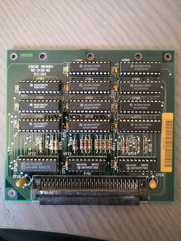
The tag RAM is 12 bits wide. So the three 4k x 4 tag SRAM chips are used as a 4k x 12 memory array. Assuming the board tags and caches individual 32-bit values, you have 4K cache lines of 32 bits each, and a 12 bit tag for each of the cache lines.
Note that the tag SRAM chips are not just 4k x 4 SRAMs, but they contain two integrated extra functions: They can be completely cleared to in a single operation taking just 70ns, and they provide an built-in comparator that provides a single output indicating whether the data presented at the data pins is identical to the data stored in the memory. Those special chips fell out of favour when chipsets got complex enough to do these operations inside the chipset, so they are hard to get nowadays.
Assuming a direct mapped cache, the cacheable area is 2^(tag bits) * cache size at max (if there is a "valid" bit inside the tag, decrement the tag bit count by one), so you get 4096 * 16k = 64M cacheable area (assuming "always valid" operation) or 32M cacheable area (assuming a dedicated valid bit). Bulk-clearable address tag comparator RAMs fit very well into a system with a dedicated valid bit. You just fix the "input" for that bit to 1, and the chip will output "no match" for all locations that have not yet been written.
If you upgrade to 64K of cache, you need two less tag bits for the same cacheable area. Assuming all 12 bits are used, you still need 10 tag bits, which means you need 3 chips of special 16k x 4 tag SRAM including an integrated comparator and bulk clear. If you can take a hit of a factor of 4 on the cacheable area by just using 8 tag bits, you might get away with 2 of those special tag SRAM chips.
I assume that the output enable signal of the tag chips is permanently grounded, causing them to never operate in "read" mode that presents the contents of the RAM on the data pins, but they keep operating in "compare" mode (outputting the match signal on a dedicated output-only pin) or "write" mode. In that case, the data pins are input-only and can be directly connected to the processor address bus (possibly buffered). The 573 chips are latch chips. I guess they are address latches that are used to finish a read/write operation while the 80386 already presents the next address due to "address pipelining". In that case, the tag chips might very well be connected to the unlatched addresses (to start the tag comparison early), while the data chips are connected to the latched addresses (to be able to handle the data late). For 4k chips, you only need 12 address bits, and for 16k chips, you need 14 address bits. The two 573 chips provide 16 latch bits, so it might be possible to go up to 256k cacheable area using a similar board design - provided you have enough unobtainium at hand to get two 64k x 4 or one 64k x 8 self-clearing tag-comparing SRAM chips, or you use a PAL to decode between multiple smaller tag SRAMs.