Reply 20 of 32, by MikeSG
MSxyz wrote on 2024-04-05, 09:59:The bad news is that the system is a bit underperforming.
[...]
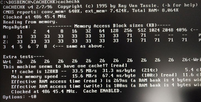
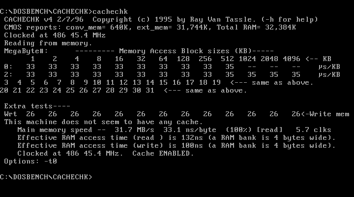
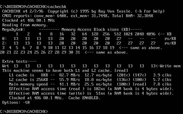
... CacheCHK doesn't seem to recognize the 2KB cache at all (see pic). Before working further on this setup, I need to dig up some old utilities for the Cyrix CPUs. The one I used for the 486DLC doesn't appear to be working with the 486S.
The RAM speed is a little slow.. should be 20-30MB/S.
L2 cache (128KB) is approx the right speed.
L1 cache is not detected...
The Cyrix app may not work on this CPU to turn on the internal cache, and the BIOS may not know how to turn on the internal cache...
If you can find the datasheet for the CPU and find the pin "KEN", then just connect GND to turn it on. If you need to guess, use a 5k resistor to GND.
This is a list of many 486 CPUs and their pins but the Cyrix SX-40 may be different to all of them. http://www.pchardwarelinks.com/486pin2.htm
Honestly it should be connected somewhere to either the interposer or the motherboard.