Reply 40 of 275, by Scali
wrote:My opinion is that these chips weren't intended to work with advanced buses or maybe Yamaha just saved on silicon/pin count. These chips were initially intended for various cost-sensitive 8-bit systems and I don't think you can do much useful work on these CPUs, overlapped with OPL register writes.
Well, if you look at the OPL2, it requires 35 IO cycles of delay after a data write.
Even on an 8088 at 4.77 MHz, an IO cycle is 4 CPU cycles, so that means that you are wasting 140 CPU cycles for every data write. That would be more than enough to 'camouflage' the overhead of a timer interrupt.
So by not stalling the CPU, you could in theory use a timer interrupt to periodically write to the OPL2 chip in the background.
On CPUs with lower interrupt overhead, such as a 6502, it is even more in the favour of the CPU.
And that's the theoretical best case.
If you would do 35 dummy reads on an 8088 at 4.77 MHz in practice (like most software does, since it was in the AdLib programming manual), each read instruction would take far more than just 4 CPU cycles, probably more like 10. So you are wasting 350 CPU cycles. That's why AdLib music can be quite CPU-intensive on an 8088.
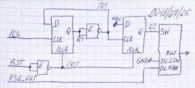
wrote:Proper solution would be to introduce hw that delays the next access until timeout has expired. I'm not sure this would stop the CPU that just performed a single write operation.
That could work, but was probably too complex/costly to implement back in the day. OPL2/3 are of course very low-budget FM synth chips in Yamaha's product range.
It would be the ideal case if the delay would be taken before the next write. Because the write itself is latched inside the OPL2, so it completes immediately after the bus transfer. The latched value just needs to kept from being overwritten until the chip has finished processing the new state.
But as said, no software and no hardware works like that, so introducing something like that today is rather useless now.


