VOGONS


Voodoo 1 vs. Voodoo 2 on a 486

Topic actions

Reply 80 of 124, by Scali

User metadata
Rank l33t
Rank
l33t
feipoa wrote:

That is pretty intersting. What I don't really understand is how the logic works to re-order the instructions. This logic is presumably hardware-based and on the CPU itself. I would imagine it is quite complex, but what's the crux of the alogrythm? Is it like a little ASIC in the CPU dye? Also, to reorder the instructions, the CPU must gather multiple instrutions for the reordering. What exactly does this mean? Are there, for example, a half-dozen instructions layed out in the pipeline, probably in a shift register, then get reordered within that shift register? And what ordering would be optimal? It is a fascinating subject that I wish I knew more about from a high-level perspective.

The CPU is basically 'split in two'.
The first part decodes instructions into a buffer, into what is commonly known as 'micro ops'. These are simple RISC-like instructions for the internal execution pipeline.
The second part contains a scheduler. This is basically a sort of 'scoreboarding' where the CPU keeps track of which operands and execution units are ready for execution.
So the CPU will constantly scan the buffer of decoded instructions for instructions that it can execute. The order is basically determined by availability of the resources. It is not necessarily the 'optimal' ordering for the entire program, but it is reasonably optimal for the instructions in the window.

This makes optimizing for these CPUs an interesting problem: instead of trying to reduce your algorithm to the minimum number of instructions, you now need to think about the out-of-order logic. Two things are important:
1) Use the simplest encoding of instructions whenever possible (some x86 instructions map 1:1 to micro ops, others decode into multiple dependent micro ops, taking more resources both for decoding and execution).
2) Reduce dependencies of instructions on previous results to a minimum. The CPU only has a limited 'window' of instructions it can pre-decode and buffer, so the input for the out-of-order logic is limited. If you fill the buffer with instructions that each depend on the previous one, then it cannot take advantage of instruction-level parallelism.

Hyperthreading is a clever trick to make 2) more efficient: By decoding not one but two (or more) threads at the same time, you have a lot more independent instructions to choose from. Instructions from different threads are independent by definition.

http://scalibq.wordpress.com/just-keeping-it- … ro-programming/

Reply 81 of 124, by dirkmirk

User metadata
Rank Oldbie
Rank
Oldbie

It looks like the POD83/AM5X86-160/CX5X86-120/133 are ballpark, the AMD edges out the Cyrix in some benchmarks the Cyrix 133 in others, the POD83 in others.

As an all round CPU the AM5X86 is a bargain, the IBM5X86C is comparable to a POD83, the Cyrix 133 is not worth it IMO, if it was a 150 or 160mhz part it would be excellent but personally I dont think the prices are justified its purely based on rarity.

Reply 83 of 124, by feipoa

User metadata
Rank l33t++
Rank
l33t++

Thanks for the additional explanation. Any idea how many opcodes fit into this buffer on a cx5x86? Is the ordering alogrythm rather simple then, that is, if it is only looking at availability of resources? So are the instructions to be executed based on what hardware has just freed up, e.g. a shift register, counter, FPU unit, comparator, etc, so that one instruction is hopefully not waiting around for the next? What happens, then, when you add branch prediction to this scheme? Is it that instruction are no longer executed based on available resources, but on what instruction may be needed next to avoid waiting (branch hit)?

Is it that the compiler hands over assembly code to the CPU and the CPU then turns the assembly into opcode (e.g. ADD into 0x1F)? Or is the RISC-like instructions you mention something between Assembly and the hex-represented opcode? Or the CPU turns the assembly into 32-bit binary, whereby the first 8 bits (of that 32-bit string) may represent the opcode? It is these opcodes which get executed based on available resources?

I noticed that branch prediction on the Cyrix 5x86 didn't help all that much when it came to 3D accelerated games. In Quake, for example, branch prediction (BTB) added about 2-3%, while in synthetic benchmarks, branch prediction improves results beyond 50%. Out of order execution (LSSER) adds 7% to Quake.

dirkmirk wrote:

It looks like the POD83/AM5X86-160/CX5X86-120/133 are ballpark, the AMD edges out the Cyrix in some benchmarks the Cyrix 133 in others, the POD83 in others.

As an all round CPU the AM5X86 is a bargain, the IBM5X86C is comparable to a POD83, the Cyrix 133 is not worth it IMO, if it was a 150 or 160mhz part it would be excellent but personally I dont think the prices are justified its purely based on rarity.

The benefit of the Cyrix 5x86-133 is the standard front-side and PCI bus speed. Some PCI cards don't like 40 MHz. Some boards force 27 MHz onto the PCI bus for 40 MHz FSB's. Some systems might not work with the fastest timings at 40 MHz, which will really hurt. There are a lot of IFs, which make 33 MHz simpler. But then again, some older motherboards might not work with the Cyrix LSSER feature, which plays a major role in its performance benefit. For non-graphic tasks, the AM5x86-160 looses the benefit of its 40 MHz PCI bus. As for POD83, finding a motherboard to work properly with L1 WB is a challenge. I think sometimes CHKCPU reports L1 in WB, but it has the performance of WT, so testing is necessary.

It would be fun to run a similar 3D game comparison in a non-graphic card accelerated mode.

I have noticed that some Am5x86-133 chips do not run well at 160 MHz with the motherboard's standard 3.3 V. Often 3.45 V - 3.6 V was required for prolonged stability.

So far, I have only had luck with the QFP versions of the IBM 5x86c chips at 133 MHz. One or two others on the forum, though, said that are able to run the PGA variants at 133 MHz. I killed one of my QFP IBM 5x86c chips testing for 150 MHz. It ran very well while it ran, then just wouldn't turn on any more. Perhaps I'll try another one one of these days. I'm sure there must be one out there to work at 150 MHz. Just one maybe...

Plan your life wisely, you'll be dead before you know it.

Reply 84 of 124, by feipoa

User metadata
Rank l33t++
Rank
l33t++
AtTheGates wrote:

I'm impressed you could even get 7FPS in Unreal with a 486.

The frame rate feels a lot faster when playing the game walking through that crashed space ship, if that is what it is.

It would be nice to see how other systems perform. I have run things pretty well optimised and suspect not all other systems can follow suit.

Plan your life wisely, you'll be dead before you know it.

Reply 85 of 124, by Logistics

User metadata
Rank Oldbie
Rank
Oldbie

As everyone has reiterated, time and time again, the limiting factor is the CPU. Realistically, the best you can do to improve Voodoo 1 performance is to make the rest of the system ultra-stable. This means replacing the capacitors in the power supply with new, quality capacitors, same for the motherboard, and if your particular Voodoo 1 had small electrolytics, those too! Essentially, you have to do the same for any sound card you're using to make sure it keeps pace with your other hardware as best as it possibly can--really, just the electrolytics which are tied to the incoming power traces, i.e. +5V, +12V, etc.

If you're using a CRT monitor, I would highly, suggest you find yourself a VGA cable that you know, for a fact, has been constructed with true, 75-Ohm mini-coax on the Red, Blue, Green and H-Sync and V-Sync lines. You'll benefit from a richer, more stable picture.

Reply 86 of 124, by Scali

User metadata
Rank l33t
Rank
l33t
feipoa wrote:

Thanks for the additional explanation. Any idea how many opcodes fit into this buffer on a cx5x86?

I have no idea how the Cyrix 5x86 works exactly. As far as I understand, it can only reorder loads and stores, but it is not clear how it does that.
Since it is not a full out-of-order-execution CPU, I doubt that they actually go through the trouble of decoding and buffering instructions.
My guess is that they simply implemented some 'shortcuts' in the pipeline. Even the Pentium has that, for example with the LEA instruction. This is executed one stage earlier in its pipeline than regular ALU instructions.
So I would suspect that the 5x86 can process loads and stores perhaps a few stages earlier than the ALU, and that would give them a few cycles to reorder them (possibly combining a store and a load to the same address?).
All I could find on it is this: https://web.archive.org/web/20030104144558/ht … .com/5x-tb.html

The advanced load/store unit is capable of managing concurrent operations and processing loads and stores out of order while maintaining a three-deep load queue and four-deep store queue.

So it seems it can queue up 3 loads and 4 stores internally.

feipoa wrote:

Is the ordering alogrythm rather simple then, that is, if it is only looking at availability of resources?

Well, it's not quite THAT simple in practice, Pentium Pro already had register renaming as well, and there are various other small details and optimizations of course. But the basis is indeed just picking whichever instruction is ready for execution, based on the availability of its operands, and an execution unit that is compatible.

feipoa wrote:

What happens, then, when you add branch prediction to this scheme? Is it that instruction are no longer executed based on available resources, but on what instruction may be needed next to avoid waiting (branch hit)?

Well, the idea of predicting a branch is just that you 'pick a side' and basically eliminate the branch from the execution path. So the prediction logic just decides which side to pick, and the CPU continues executing as normal, picking the instructions from the path that it had predicted. There's a simple 'rollback' implemented in case the branch turns out wrong (at the point the branch is actually executed, and the result is known).

feipoa wrote:

Is it that the compiler hands over assembly code to the CPU and the CPU then turns the assembly into opcode (e.g. ADD into 0x1F)? Or is the RISC-like instructions you mention something between Assembly and the hex-represented opcode? Or the CPU turns the assembly into 32-bit binary, whereby the first 8 bits (of that 32-bit string) may represent the opcode? It is these opcodes which get executed based on available resources?

Hum, I think we need to have a few definitions first:
Assembly code is human-readable code. An assembler converts this code to machine code. A CPU executes machine code.
The confusion here is that x86 CPUs are designed to execute x86 machine code. This code however dates from the 1970s, and is very complex in nature (variable length encoding, implicit operands etc).
To make out-of-order execution more efficient, these x86 instructions are translated to an internal representation. This can be seen as another type of machine code. You could say that modern x86 CPUs are 'emulating' an x86 instructionset by translating the code on-the-fly.

These internal representations are proprietary, and as far as I know, no manufacturer has ever published what their internal representation looks like exactly. But roughly, yes, they would have chosen a very simple and efficient encoding (RISC-like), probably all instructions the same size, and simple groups of bits to indicate operands etc.

http://scalibq.wordpress.com/just-keeping-it- … ro-programming/

Reply 87 of 124, by feipoa

User metadata
Rank l33t++
Rank
l33t++
Scali wrote:

To make out-of-order execution more efficient, these x86 instructions are translated to an internal representation. This can be seen as another type of machine code. You could say that modern x86 CPUs are 'emulating' an x86 instruction set by translating the code on-the-fly.

These internal representations are proprietary, and as far as I know...

Now that catches my curiosity and things sorta make more sense now. So the CPU cannot decode assembly at all? I remember back in the mid 90's, when you wrote a program or game for a TI-85 calculator, for example, if you wrote it in assembly, the program would run so so much faster than using the calculator's BASIC language, which it had to compile. So the calculator's CPU, or some feature within the CPU, isn't translating the assembly to machine code (1's and 0's).

Most of the information I could find on the Cyrix 5x86's architecture is found in these two PDFs, http://datasheets.chipdb.org/Cyrix/5x86/5X-DPAPR.PDF and http://datasheets.chipdb.org/Cyrix/5x86/5X-ABDB.PDF

Items concerning out-of-order execution, branch prediction, and parallelism are quoted here:

The Cyrix 5x86 family represents a new generation of x86-compatible 64-bit microprocessors with fifth-generation features. The B […]
Show full quote

The Cyrix 5x86 family represents a new generation of x86-compatible 64-bit microprocessors with fifth-generation features. The Branch Target Buffer provides branch prediction with accuracy averaging 80%. The decoupled Load/Store unit allows multiple instructions in a single clock cycle. Other features include single-cycle execution, single-cycle instruction decode, 16-KByte Write-Back cache, and clock rates up to 120 MHz made possible by the use of advanced process technologies and superpipelining.
...
Instruction fetch... Up to 128 bits of code are read during a single clock cycle.
...
The memory management unit also contains a load/store unit that is responsible for scheduling cache and external memory accesses. The load/store unit incorporates two performance-enhancing features:
• Load-store reordering that prioritizes memory reads required by the integer unit over writes to external memory
• Memory-read bypassing that eliminates unnecessary memory reads by using valid data still in the execution unit.
...
The 5x86 processor floating point unit interfaces to the integer unit and the cache unit through a 64-bit bus. The 5x86 CPU FPU is x87-instruction-set compatible and adheres to the IEEE-754 standard. Because most applications contain FPU instructions mixed with integer instructions, the 5x86 FPU achieves high performance by completing integer and FPU operations in parallel. FPU instructions are dispatched to the pipeline within the integer unit. The address calculation stage of the pipeline checks for memory management exceptions and accesses memory operands for use by the FPU. Once the instructions and operands have been provided to the FPU, the FPU completes instruction execution independently of the integer unit.
...
The memory management unit contains a 32-entry translation lookaside buffer, a load/store unit capable of managing concurrent operations, and the address calculation unit. The 5x86 functional units are interconnected by two 32-bit busses that permit non-blocking operation of the units. A 128-bit instruction fetch bus feeds 16 bytes of code per cycle to a three-line deep buffer in the instruction decode unit.
...
The cache data port is 64 bits wide and can be split into two 32-bit data paths. The ability to have two 32-bit data paths allows the 5x86 to simultaneously perform a 32-bit data transfer to or from main memory, and a 32-bit data transfer to or from the load/store unit. In addition, superpipelining the 5x86 address calculation stage allows cache accesses in a single clock cycle, identical to register accesses.
...
Correctly predicted branch instructions execute in a single clock. Incorrectly predicted branches require five clock cycles to flush the instruction pipeline....
The 5x86 CPU implements an advanced load/store unit to reduce the typical bottlenecks associated with load/store processing. The pipelined load/store unit is capable of managing concurrent operations and of processing loads and stores out of order while maintaining a three-deep load queue and four-deep store queue. The load/store unit is also responsible for handling all read/write requests from the address calculation unit, managing read-afterwrite dependencies for memory accesses, performing data forwarding, and checking self modifying code.
...
The address calculation stage of the pipeline checks for memory management exceptions and accesses memory operands for use by the FPU. The load/store unit is responsible for managing FPU operands. Once the instructions and operands have been provided to the FPU, the FPU completes instruction execution independently of the ALU and load/store unit

I wasn't aware that the Pentium didn't contain out-of-order execution logic. The two games in which the Pentium really jumped ahead was Quake and Hexen II. So the coding and compiling of these games was deliberately written in an optimal order for the Pentium's architecture?

Plan your life wisely, you'll be dead before you know it.

Reply 88 of 124, by Scali

User metadata
Rank l33t
Rank
l33t
feipoa wrote:

Now that catches my curiosity and things sorta make more sense now. So the CPU cannot decode assembly at all? I remember back in the mid 90's, when you wrote a program or game for a TI-85 calculator, for example, if you wrote it in assembly, the program would run so so much faster than using the calculator's BASIC language, which it had to compile. So the calculator's CPU, or some feature within the CPU, isn't translating the assembly to machine code (1's and 0's).

Yes, it would have assembled the source to machine code in software, before the CPU could execute it.
Since assembly is so much more lowlevel than BASIC, it is much faster to convert it to machine code, and the resulting code will usually run much faster as well.

feipoa wrote:

I wasn't aware that the Pentium didn't contain out-of-order execution logic. The two games in which the Pentium really jumped ahead was Quake and Hexen II. So the coding and compiling of these games was deliberately written in an optimal order for the Pentium's architecture?

Well, I can speak for Quake, which was very specifically hand-optimized for the Pentium.
It took advantage of the two pipelines by manually pairing instructions in assembly. It also took advantage of the asynchronous FPU, firing off a division in the background, and running integer code in the foreground, until the result of the division was present. This makes the perspective divide in the texture mapper virtually 'free' on the Pentium.
This also explains why Quake gets such poor performance on a 486: its FPU is not capable of this.
Descent is an excellent example of a game that was specifically optimized for the 486.

I don't know the specifics of Hexen II, but it runs on a modified Quake engine, so I suppose the basic Pentium optimizations are still there.

http://scalibq.wordpress.com/just-keeping-it- … ro-programming/

Reply 89 of 124, by leileilol

User metadata
Rank l33t++
Rank
l33t++

Hexen II's still got the same assembly optimizations yes, only this time they dropped the nasm2masm conversion step since DOS got dropped anyhow for a MSVC build only.

The drawspans16 assembly routine is most of interest towards Pentium optimization. The C versions (not used by default and must be explicitly compiled to use) don't cater for Pentium and are quite a bit slower, particularily because there's no 16 pixel C DrawSpans (8 pixel only) and it's not very unrolled. GLQuake and GLHexen2 doesn't use the assembly drawing routines for obvious reasons though, sound painting/mixing ASM still matters.

apsosig.png
long live PCem

Reply 90 of 124, by feipoa

User metadata
Rank l33t++
Rank
l33t++

Heh, makes me wonder if Quake could be optimised for the Cyrix 5x86 such that it out performs the Pentium. If you look at the chart for Descent 2, the POD83 is third from the bottom, yet in Quake, the POD83 is at the top.

Also makes me wonder if any software was optimised for the cx5x86. This CPU was around for such a short time that it seems unlikely. The cx6x86, on the other hand, is superscalar so optimisations for it may not apply to the cx5x86 so well.

Plan your life wisely, you'll be dead before you know it.

Reply 91 of 124, by Scali

User metadata
Rank l33t
Rank
l33t
feipoa wrote:

Heh, makes me wonder if Quake could be optimised for the Cyrix 5x86 such that it out performs the Pentium.

Most probably not. The Pentium is a pure powerhouse when you optimize your code for it. It's like 2 486es tied together, but with faster execution units, better cache, and a superior FPU.
The 5x86 is more of a slightly tweaked 486 core. I don't think specific optimizations will gain much over running regular optimized 486/Pentium code.
Given that the 5x86 FPU can run in parallel with integer code, it should already benefit from the Pentium fdiv optimizations in Quake. That might explain why it performs better than other 486-like CPUs.

http://scalibq.wordpress.com/just-keeping-it- … ro-programming/

Reply 92 of 124, by feipoa

User metadata
Rank l33t++
Rank
l33t++
Scali wrote:

That might explain why it performs better than other 486-like CPUs.

Yes, and it was most noticeable in Quake/Hexen2. Do none of the other games tested make use of this particular optimisation?

Plan your life wisely, you'll be dead before you know it.

Reply 93 of 124, by AtTheGates

User metadata
Rank Newbie
Rank
Newbie
feipoa wrote:
AtTheGates wrote:

I'm impressed you could even get 7FPS in Unreal with a 486.

The frame rate feels a lot faster when playing the game walking through that crashed space ship, if that is what it is.

It would be nice to see how other systems perform. I have run things pretty well optimised and suspect not all other systems can follow suit.

Well count me out. I only have a 20Mhz 486! 😁

Reply 94 of 124, by feipoa

User metadata
Rank l33t++
Rank
l33t++

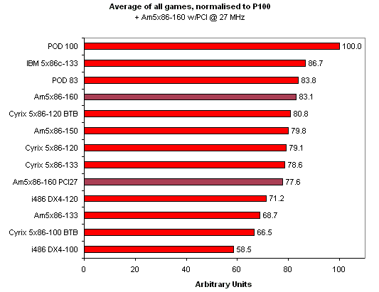
I decided to measure and include results for the situation whereby the Am5x86-160 is run with a 26.7 MHz PCI bus instead of a 40 MHz FSB. This might be done deliberately by the user for expansion card compatibility, or by absolute insistence of the BIOS. Concerning the latter case, the PC Chips M919 imposes a 2/3 * FSB multiplier if you are running the front-side bus at 40 MHz. This imposition is automatic and hidden from sight. The inconvenient work around is to boot with a 33 MHz FSB, then switch the FSB jumper to 40 MHz after POST.

The performance hit with the 27 MHz PCI bus was moderate at about 7%. The GLQuake score reduced to equal that of the Am5x86-150, and in nearly all other cases, the Am5x86-160-PCI27 results were 2-3% worse than the Am5x86-150.

Average_all_games_normalised_to_POD100_plus_Am5x86-160-PCI27.png
Filename
Average_all_games_normalised_to_POD100_plus_Am5x86-160-PCI27.png
File size
8.08 KiB
Views
1269 views
File license
Fair use/fair dealing exception

Plan your life wisely, you'll be dead before you know it.

Reply 96 of 124, by AtTheGates

User metadata
Rank Newbie
Rank
Newbie
feipoa wrote:

I decided to measure and include results for the situation whereby the Am5x86-160 is run with a 26.7 MHz PCI bus instead of a 40 MHz FSB. This might be done deliberately by the user for expansion card compatibility, or by absolute insistence of the BIOS. Concerning the latter case, the PC Chips M919 imposes a 2/3 * FSB multiplier if you are running the front-side bus at 40 MHz. This imposition is automatic and hidden from sight. The inconvenient work around is to boot with a 33 MHz FSB, then switch the FSB jumper to 40 MHz after POST.

The performance hit with the 27 MHz PCI bus was moderate at about 7%. The GLQuake score reduced to equal that of the Am5x86-150, and in nearly all other cases, the Am5x86-160-PCI27 results were 2-3% worse than the Am5x86-150.

Average_all_games_normalised_to_POD100_plus_Am5x86-160-PCI27.png

What is "POD"?

Reply 98 of 124, by feipoa

User metadata
Rank l33t++
Rank
l33t++

POD = Pentium Overdrive. It is a Pentium CPU which fits into a 486 motherboard's socket 3. 83 = 83 MHz, 100 = 100 MHz.

Plan your life wisely, you'll be dead before you know it.